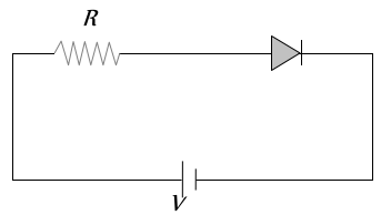
In a forward biased $P N$-ju nction diode, the potential barrier in the depletion region is of the form ...
- A
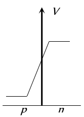
- B
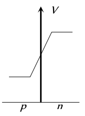
- C
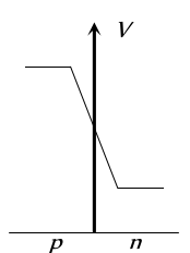
- D
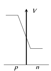
[KCET 2004]


Download our appand get started for free
Experience the future of education. Simply download our apps or reach out to us for more information. Let's shape the future of learning together!No signup needed.*
Similar Questions
- 1View SolutionIn comparison to a half wave rectifier, the full wave rectifier gives lower
- 2In a $P N P$ transistor working as a common-base amplifier, current gain is $0.96$ and emitter current is $7.2\ mA$. The base current isView Solution
- 3View SolutionIn case of a semiconductor, which of the following statement is wrong
- 4$P$-type semiconductor is formed whenA. As impurity is mixed in $S i$B. $A$ Impurity is mixed in $S i$C. $B$ impurity is mixed in $G e$D. $P$ impurity is mixed in $G e$View Solution
- 5In a $P$-type semiconductor, germanium is doped withView Solution
- 6View SolutionAt ordinary temperatures, the electrical conductivity of semi conductors in mho/meter is in the range
- 7For the given circuit of $P N$-junction diode, which of the following statement is correctView Solution
- 8Following is the relation between current and charge $I=A T^2 e^{q t / V_L}$ then value of $V$ will beView Solution
- 9The curve between the work function of a metal $\left(\phi_o\right)$ and its temperature $(T)$ will beView Solution
- 10In the $C B$ mode of a transistor, when the collector voltage is changed by $0.5$ volt. The collector current changes by $0.05\ mA$. The output resistance will beView Solution