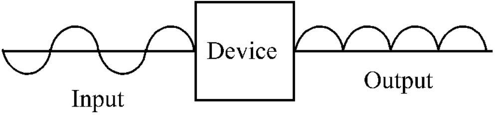
Questions

3 Marks Question

Take a timed test

7 questions · self-marked practice — reveal the answer and mark yourself.

Question 13 Marks
What is called P-N junction? Name the methods of making P-N junction. Explain the diffusion method of making $P - N$ junction.
Answer
P-N Junction: If P and N type semiconductors are joined together and kept in such a way that the atoms of the contact plane come together, then the contact plane formed in this way is called $P - N$ junction. There are three methods of making P-N junction :
(1) Growth
(2) Diffusion
(3) Metal Mixture.
Diffusion method of making P-N junction : In this at high temperature in a muffle furnace, impurity semiconductor is formed by bringing the intrinsic semiconductor wafer with appropriate impurity in contact with steam. The impurity semiconductor thus obtained is now known as the opposite impurity diffusion is caused by bringing atoms (P-type semiconductor with V-group element and Ntype semiconductor with III-group element) in contact. The amount of diffusion decreases with depth. As a result, as far as there are impurities in the crystal, joints are present there.
View full question & answer
Question 33 Marks
Classify metals, conductors and semiconductors.
Answer
On the basis of conductivity : On the basis of relative value of electrical conductivity ( $\sigma$ ) or resistivity $( \rho=$
$1 / \sigma$ ) solid materials are classified as follows :
$(i)$ Metals : Their resistivity is very low $($or conductivity is very high$).$
$\rho \sim 10^{-2}-10^{-8} \Omega m$
$\sigma \sim 10^2-10^8 Sm^{-1}$
$(ii)$ Semiconductors : Their resistivity or conductivity is between metals and insulating materials.
$\rho \sim 10^{-5}-10^6 \Omega m$
$\sigma \sim 10^5-10^{-6} Sm^{-1}$
$(iii) $ Insulators : Their resistance is very high $($or conductivity is very low$).$
$\rho \sim 10^{11}-10^{19} \Omega m$
$\sigma \sim 10^{-11}-10^{-19} Sm^{-1}$
The values of $\rho$ and $\sigma$ given above are only indicative of the order value and may go outside the given range.
View full question & answer
Question 43 Marks
Explain the difference between conductor, insulator and semiconductor on the basis of energy band in solids.
Answer
On the basis of energy band, the difference between conductor, insulator and semi-conductor is divided as follows :
(i) Conductors: Those substances for which the forbidden energy gap $\Delta E$ is almost zero, are called conductors. In these the valence band and conduction band overlap each other.
(ii) Insulators: Those substances for which the value of forbidden energy gap $\Delta E g$ situated between the valence band and conduction band is 6 eV or more, are called insulators or insulators.
(iii) Semiconductor : Those substances for which the value of forbidden energy gap between valence band and conduction band is around 1 eV , they are called semiconductor materials.
View full question & answer
Question 53 Marks
What is called extrinsic semiconductor? Explain doping process.
Answer
Extrinsic semiconductor : The conductivity of intrinsic semiconductors is very low at room temperature. Therefore, to increase the conductivity, a small amount of certain element of the third or fifth group is added to the semiconductor. The semiconductor obtained in this way is called impurity semiconductor or extrinsic semiconductor.
Doping : The process of introducing impurity atoms into a intrinsic semiconductor is called doping.
To obtain extrinsic semiconductor, approximately from $(10)^6$ to $(10)^{10}$ atoms are one atom is of impurity element in intrinsic semiconductor.
View full question & answer
Question 63 Marks
What are valence band and conduction band? Define forbidden energy gap.
View full question & answer
Question 73 Marks
Define semiconductors on the basis of energy band theory. What are the charge carriers in semiconductor? What do semiconductors start behaving like at absolute zero temperature?
Answer
Semiconductor : Those substances for which the value of forbidden energy gap is about 1 eV , are called semiconductors. For example, this gap is 1.1 eV for $Si , 0.7$ eV for Ge and 1.3 eV for gallium arsenide. In semiconductors, electrons and holes act as charge carriers. The resistivity and conductivity of semiconductors are between conductors and insulators. At room temperature, some electrons get excited by thermal energy and move from the valence band to the conduction band and conduct a certain amount of electric current.
At absolute zero temperature the thermal energy of electrons is zero, hence their motion is restricted. Therefore, a semiconductor is unable to conduct current in the presence of an external electric field and behaves like a bad conductor. The resistance temperature coefficient of semiconductors is negative.
View full question & answer