Gujarat BoardEnglish MediumSTD 12 SciencePhysicsSEMICONDUCTOR ELECTRONICS: MATERIALS, DEVICES AND SIMPLE CIRCUITS3 Marks
Question
Explain how $p-n$ junction is formed.
✓
Answer
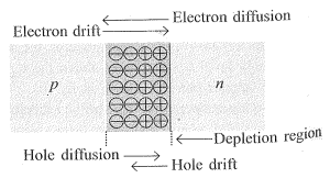
→Consider a thin $p$-type silicon $(p- S i)$ semiconductor wafer. By adding precisely a small quantity of pentavalent impurity, part of the $p$ - Si wafer can be converted into $n- S i$. →The wafer now contains $p$-region and $n$-region and a metallurgical junction between $p$ and $n$-regions. →Two important processes occur during the formation of a $p-n$ junction: (1) diffusion (2) drift →In an $n$-type semiconductor, the concentration of electrons (number of electrons per unit volume) is more compared to the concentration of holes. Similarly, in a p-type semiconductor, the concentration of holes is more than the concentration of electrons. During the formation of $p-n$ junction, and due to the concentration gradient across $p$ and $n$ - sides, holes diffuse from $p$ - side to $n$ - side $(p \rightarrow n)$ and electrons diffuse from $n$ - side to $p$ - side $(n \rightarrow p)$. →This motion of charge carriers gives rise to diffusion current across the junction. →When an electron diffuses from $n \rightarrow p$, it leaves behind an ionised donor on $n$ - side. The ionised donor ( $+v e$ charge) is immobile as it is bonded to the surrounding atoms. As the electrons continue to diffuse from $n \rightarrow p$, a layer of positive charge (or positive space charge region) on $n$ - side of the junction is developed. →Similarly when a hole diffuses from $p \rightarrow n$ due to the concentration gradient, it leaves behind an ionised acceptor (negative charge) which is immobile. As the holes continue to diffuse from $p \rightarrow n$, a layer of negative charge (or negative space-charge region) on the $p$-side of the junction is developed. →The space-charge region on either side of the junction together is known as depletion region as the electrons and holes taking part in the initial movement across the junction depleted the region of its free charge. (fig.) The thickness of the depletion region is of the order of onetenth of a micro-meter. →Due to the positive space-charge region on $n$-side of the junction and negative space charge region on $p$-side of the junction, an electric field directed from positive charge towards negative charge develops. Due to this field, an electron on $p$-side of the junction moves to $n$-side and a hole on $n$-side of the junction moves to $p$-side. The motion of charge carriers due to the electric field is called drift. →Thus, a drift current, which is opposite in direction to the diffusion current starts. →Initially, diffusion current is large and driftcurrent is small. As the diffusion process continues, the space-charge regions on either side of the junction extend, thus increasing the electric field strength and hence drift current. This process continues until the diffusion current equals the drift current. Thus a $p-n$ junction is formed. In a $p-n$ junction, under equilibrium, there is no net current.
Need a full question paper?
Generate a complete, print-ready paper with questions like this in minutes — across 16+ boards, with answer keys.