Holes are charge carriers in
[IIT-JEE 1996]


Download our appand get started for free
Experience the future of education. Simply download our apps or reach out to us for more information. Let's shape the future of learning together!No signup needed.*
Similar Questions
- 1In diode, when there is saturation current, the plate resistance $\left(r_p\right)$ isView Solution
- 2Electronic configuration of germanium is $2,8,18$ and $4$ . To make it extrinsic semiconductor small quantity of antimony is addedView Solution
- 3In the case of forward biasing of $P N$-junction, which one of the following figures correctly depicts the direction of flow of carriersView Solution
- 4In a $\text{PNP}$ transistor the base is the $N-$region. lts width relative to the $P-$region isView Solution
- 5The slope of plate characteristic of a vacuum diode is $2 \times 10^{-2} \ mA / V$. The plate resistance of diode will beView Solution
- 6View SolutionThe forbidden gap in the energy bands of germanium at room temperature is about
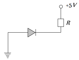
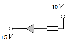
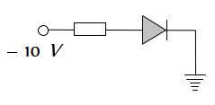
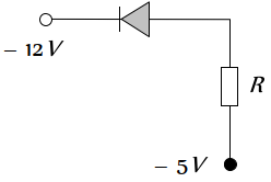
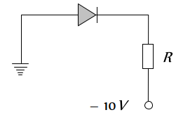
- 7View SolutionIn the given figure, which of the diodes are forward biased ?
- 8The transfer ratio of a transistor is $50.$ The input resistance of the transistor when used in the common-emitter configuration is $1 k \Omega$. The peak value for an A.C input voltage of $0.01 V$ peak isView Solution
- 9View SolutionSemiconductor is damaged by the strong current due to
- 10View SolutionA piece of semiconductor is connected in series in an electric circuit. On increasing the temperature, the current in the circuit will