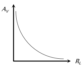
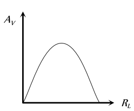
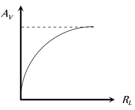
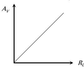
The correct curve between voltage gain $\left(A_v\right)$ and load resistance $\left(R_L\right)$ is
- A
- B
- C
- D


Download our appand get started for free
Experience the future of education. Simply download our apps or reach out to us for more information. Let's shape the future of learning together!No signup needed.*
Similar Questions
- 1Consider the following statements $A$ and $B$ and identify the correct choice of the given answers(A) A zener diode is always connected in reverse bias(B) The potential barrier of a $P N$ junction lies between $0.1$ to $0.3\ V$ approximatelyView Solution
- 2A triode has a mutual conductance of $2 \times 10^{-3} mho$ and an amplification factor of $50.$ The anode is connected through a resistance of $25 \times 10^3$ ohms to a $250$ volts supply. The voltage gain of this amplifier isView Solution
- 3No bias is applied to a $P-N$ junction, then the currentView Solution
- 4View SolutionAn oscillator is nothing but an amplifier with
- 5The slope of plate characteristic of a vacuum tube diode for certain operating point on the curve is $10^{-3} \frac{ mA }{ V }.$ The plate resistance of the diode and its nature respectivelyView Solution
- 6View SolutionZener diode is used as
- 7View SolutionThe energy band gap is maximum in
- 8View SolutionThe most commonly used material for making transistor is
- 9View SolutionIn P-type semiconductor, there is
- 10The impurity atoms which are mixed with pure silicon to make a $P$ type semiconductor are those ofView Solution