Question 11 Mark
Answer
View full question & answer→Solar cell.
46 questions · timed · auto-graded
In an n-type silicon, the electrons are the majority carriers, while the holes are the minority carriers. An n-type semiconductor is obtained when pentavalent atoms, such as phosphorus, are doped in silicon atoms.
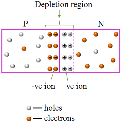
The diffusion of charge carriers across a junction takes place from the region of higher concentration to the region of lower concentration. In this case, the p-region has greater concentration of holes than the n-region. Hence, in an unbiased p-n junction, holes diffuse from the p-region to the n-region.
Of the three given elements, the energy band gap of carbon is the maximum and that of germanium is the least.
The energy band gap of these elements are related as: (Eg)C > (Eg)Si > (Eg)Ge.
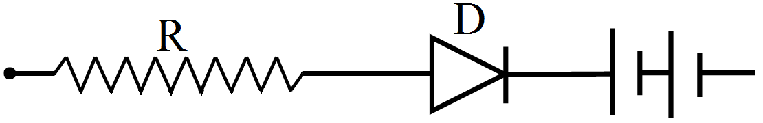
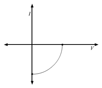
When a forward bias is applied to a p-n junction, it lowers the value of potential barrier. In the case of a forward bias, the potential barrier opposes the applied voltage. Hence, the potential barrier across the junction gets reduced.
In a p-type semiconductor, the holes are the majority carriers, while the electrons are the minority carriers. A p-type semiconductor is obtained when trivalent atoms, such as aluminium, are doped in silicon atoms.
The voltage gain of a transistor amplifier is constant at mid frequency range only. It is low at high and low frequencies.
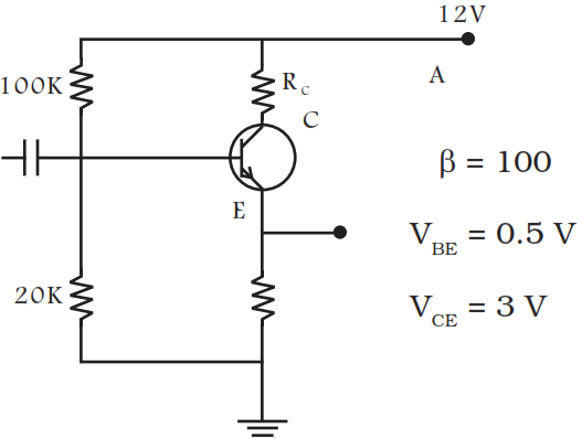
For a transistor action, the junction must be lightly doped so that the base region is very thin. Also, the emitter junction must be forward-biased and collector junction should be reversebiased.
B = 0
For beyond the horizon communication, it is necessary for the signal waves to travel a large distance. 10 KHz signals cannot be radiated effeciently because of the antenna size. The high energy signal waves (1GHz - 1000 GHz) penetrate the ionosphere. 10MHz frequencies get reflected easily from the ionosphere. Hence, signal waves of such frequencies are suitable for beyond the horizon communication. Therefore the answer is (b)