Questions

5 Marks Questions

Take a timed test

11 questions · self-marked practice — reveal the answer and mark yourself.

Question 15 Marks
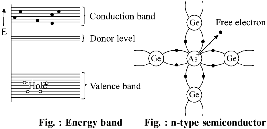
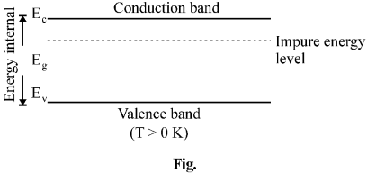
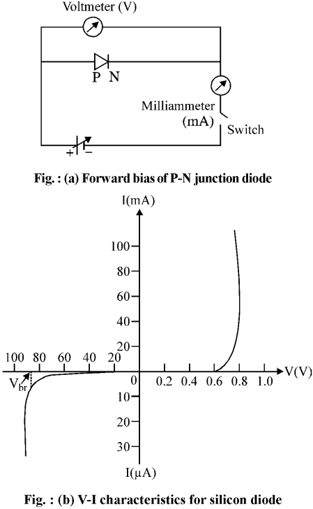
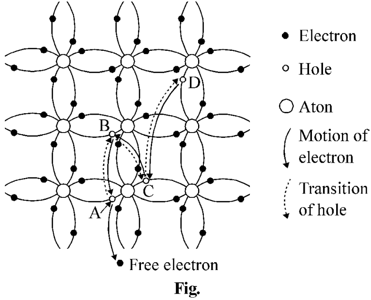
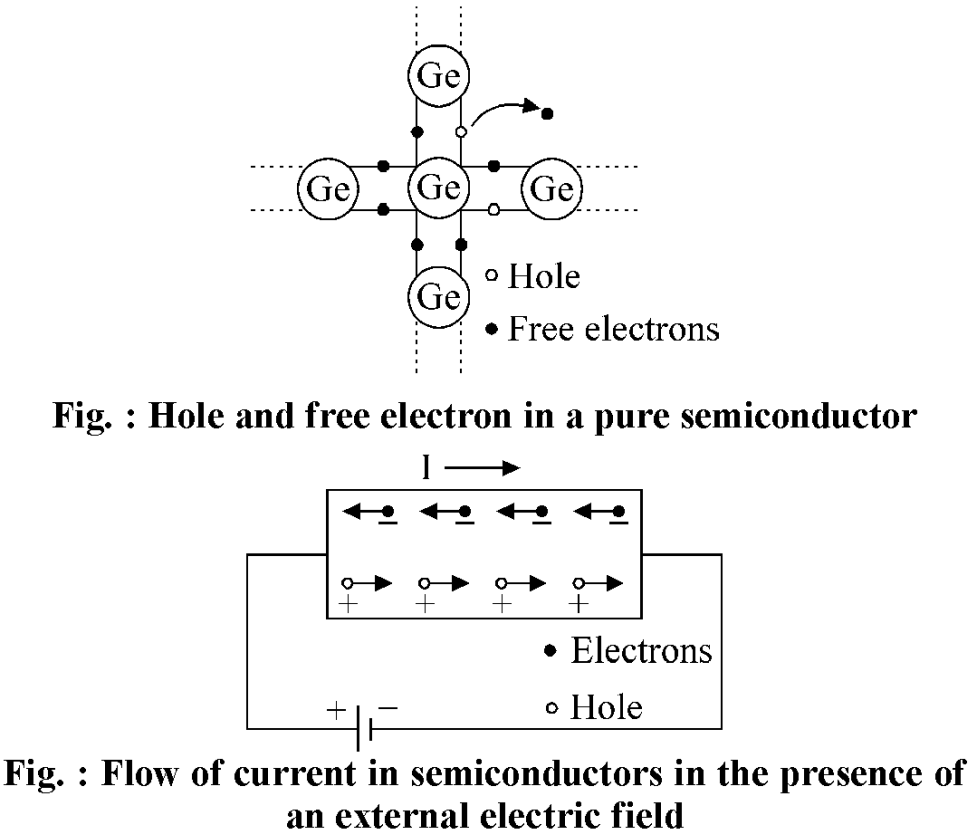
What are N-type semiconductors? Their conductivity is higher than that of pure semiconductors. Why? Explain with figure.
View full question & answer
Question 25 Marks
On the basis of band theory, differentiate between conductors, insulators and conductors.
Answer
Distinguish between Conductor, Insulator and Semi-conductor

S.No.PropertyConductorInsulatorSemi-conductor
1.Electrical conduc tivity and its valueVery high $10^{-7} mho / m$Negligible $10^{-13}$ $mho / m$In between conductor and insulator from $10^{-7} mho / m$ to $10^{-13} mho / m$
2.Resistivity and its valueNegligible less than $10^{-5} \Omega-m$Very high $10^5 \Omega- m$In between $10^{-5} \Omega- m$ to $10^5 \Omega- m$
3.Energy gap and its valueZero or minimalVery much high as in diamond $\Delta E_{g}=7 eV$More than conductors but less than insulators. For ex., in Ge , $\Delta E _{ g }=0.72 eV$ and in Si , $\Delta E _{ g }=1.1 eV$
4.Flow of current temperatureDue to free electrons and very highDue to free electrons and negligibleDue to free electrons and hole but more than insulators
5.Temperature-cofficient of resistancePositiveNegativeNegative
6.Effect on conducting on increasing tempe- ratureConductivity decreasesConductivity increases (very small increment)Conductivity increases
7.On adding impuritiesResistance increases and conductivity decreasesResistance remains unchangedResistance decreases
8.Flow of currentOccurs easilyDoes not occurVery rarely
9.ExampleCu, Ag, Au, Na, Pt and Hg etc.Wood, plastic, mica, diamond and glass etc.Ge , Si , Ga, As etc.
View full question & answer
Question 35 Marks
What is meant by rectification? Draw a diagram of a half wave rectifier electric circuit. Write a brief description of its working. Draw the waveforms of input voltage and output voltage for this rectifier circuit.
View full question & answer
Question 45 Marks
What is meant by forward bias and reverse bias of p-n junction diode? Draw experimental electrical circuit diagram to study V-I characteristic in forward bias and reverse bias of p-n junction diode. Draw forward bias and reverse bias V-I characteristic curves of p-n junction diode and briefly explain the following :
(i) Threshold or cut-in voltage
(ii) Breakdown voltage.
Answer
Forward bias : When the P end of the P-N junction is connected to the positive end of the external battery and the N end is connected to the negative end of the battery, then the P end receives higher potential than the N end. This position of the joint is said to be in forward bias junction state.
Reverse bias: When the p end of the $p - N$ junction is connected to the negative end of the battery and the N end is connected to the positive end of the battery, then the junction is called reverse biased.
Forward bias characteristic curve : In forward bias system, the curve drawn between voltage $\left( V _{ f }\right)$ and forward current $\left( I _{ f }\right)$ is called forward bias characteristic curve. To obtain the forward bias characteristic curve, a circuit is arranged as shown in the figure.
Image
Characteristic curve in Reverse Biasing : In the reverse bias system, the curve drawn in reverse voltage $\left( V _{ r }\right)$ and reverse current $\left( I _{ r }\right)$ is called reverse bias characteristic curve. To obtain the reverse bias characteristic curve, the circuit is arranged as shown.
Image
(i) Threshold or cut-in voltage : In forward bias the current initially increases very slowly to almost negligible until the voltage across the diode exceeds a certain value. After this characteristic voltage, a very small increase in the diode bias voltage results in a significant (exponential) increase in the diode current. This voltage is called threshold voltage or cut-in voltage.
(ii) Breakdown voltage: When a P-N junction diode is in the reverse biased state, a sudden increase in the value of current to a higher value is shown at a certain value of voltage, this potential is called breakdown voltage or Zener voltage. This high value current can destroy a simple P-N junction.

View full question & answer
Question 55 Marks
Draw the complete I-V characteristic curve for an ideal P-N junction diode. Define the dynamic resistance in the forward bias state.
View full question & answer
Question 65 Marks
Explain the concept of energy bands with a figure.
View full question & answer
Question 75 Marks
View full question & answer
Question 85 Marks
Describe the procedure for obtaining V-I characteristic curve in forward bias of P-N junction diode. Make a circuit diagram of the experimental arrangement.
View full question & answer
Question 95 Marks
In a semiconductor, electrons and holes move in opposite directions to each other. How? Explain with figure.
View full question & answer
Question 105 Marks
Explain graphically the flow of current in semiconductors in the presence of an external electric field.
View full question & answer
Question 115 Marks
With the help of circuit diagram, explain the working of junction diode as a full wave rectifier. Draw its input and output waveforms. Which characteristic property of junction diode makes it suitable for rectification?
Answer
Characteristic property of junction diode : In the V-I characteristic of a junction diode, we see that it allows electric current to flow only when it is forward biased.
View full question & answer