Question 515 Marks
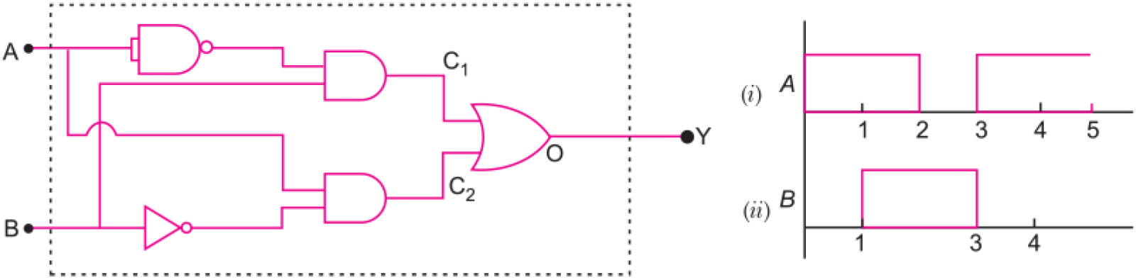
Input signals A and B are applied to the input terminals of the ‘dotted box’ set-up shown here. Let Y be the final output signal from the box.
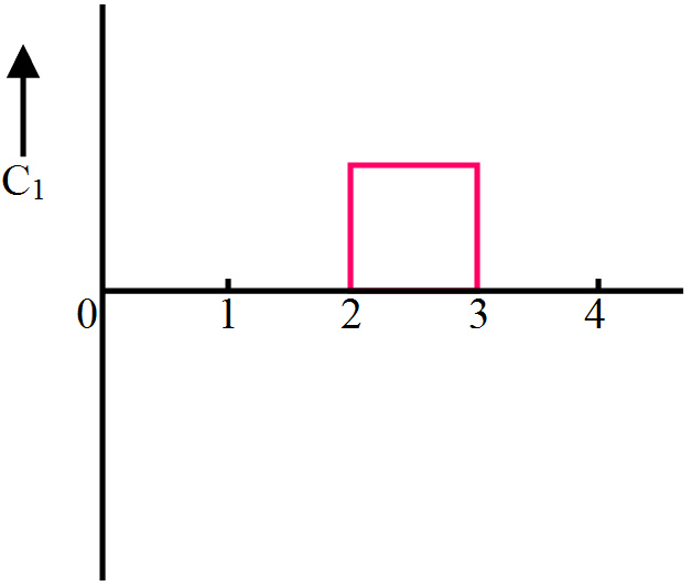
Draw the wave forms of the signals labelled as $C_1$ and $C_2$ within the box, giving (in brief) the reasons for getting these wave forms. Hence draw the wave form of the final output signal Y. Give reasons for your choice.
What can we state (in words) as the relation between the final output signal Y and the input signals A and B?
Answer
$\text{C}_1=\bar{\text{A}}\cdot\text{B},\text{C}_2=\text{A}\cdot\bar{\text{B}}$
$\text{Y}=\text{C}_1\bar+\text{C}_2=\bar{\text{A}}\text{B}\bar+\bar{\text{B}}\text{A}$
This is Boolean expression for NOT XOR gate.
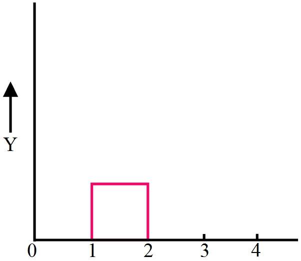
$\text{C}_1=\bar{\text{A}}\cdot\text{B}$
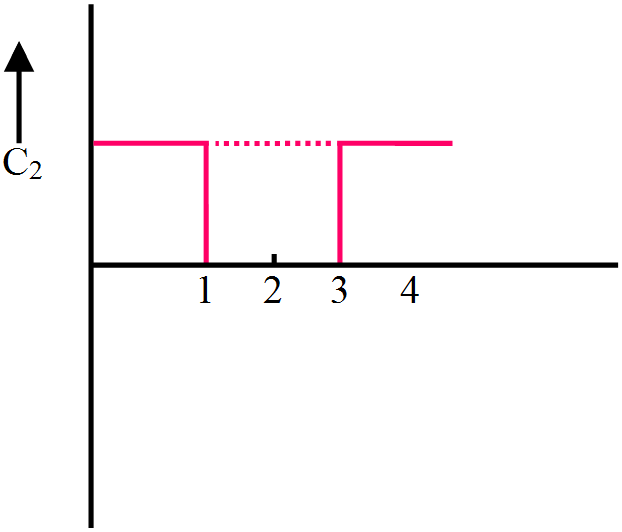
$\text{C}_2=\text{A}\cdot\bar{\text{B}}$
$\text{Y}=\text{C}_1\bar+\text{C}_2$
The gate shown in circuit is NOT XOR gate. According to definition the output Y is obtained only if either both signals are 0 or 1.
View full question & answer→$\text{C}_1=\bar{\text{A}}\cdot\text{B},\text{C}_2=\text{A}\cdot\bar{\text{B}}$
$\text{Y}=\text{C}_1\bar+\text{C}_2=\bar{\text{A}}\text{B}\bar+\bar{\text{B}}\text{A}$
This is Boolean expression for NOT XOR gate.
$\text{C}_1=\bar{\text{A}}\cdot\text{B}$
|
|
A
|
B
|
$\text{C}_1=\bar{\text{A}}\cdot\text{B}$
|
|
From 0 to 1
|
1
|
0
|
0
|
|
From 1 to 2
|
1
|
1
|
0
|
|
From 2 to 3
|
0
|
1
|
1
|
|
From 3 to 4
|
1
|
0
|
0
|
|
From 4 onwards
|
1
|
0
|
0
|
$\text{C}_2=\text{A}\cdot\bar{\text{B}}$
|
|
A
|
B
|
$\text{C}_2=\bar{\text{B}}\cdot{\text{A}}$
|
|
From 0 to 1
|
1
|
0
|
1
|
|
From 1 to 2
|
1
|
1
|
0
|
|
From 2 to 3
|
0
|
1
|
0
|
|
From 3 to 4
|
1
|
0
|
1
|
|
From 4 onwards
|
1
|
0
|
1
|
$\text{Y}=\text{C}_1\bar+\text{C}_2$
|
|
A
|
B
|
$\text{Y}=\text{C}_1\bar+\text{C}_2$
|
|
From 0 to 1
|
0
|
1
|
0
|
|
From 1 to 2
|
0
|
0
|
1
|
|
From 2 to 3
|
1
|
0
|
0
|
|
From 3 to 4
|
0
|
1
|
0
|
|
From 4 onwards
|
0
|
1
|
0
|
The gate shown in circuit is NOT XOR gate. According to definition the output Y is obtained only if either both signals are 0 or 1.