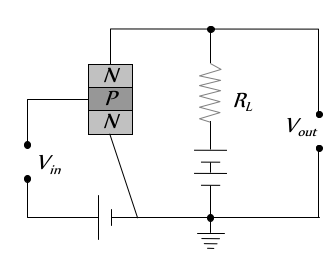
An NPN-transistor circuit is arranged as shown in figure. It is
[BHU 1994]


Download our appand get started for free
Experience the future of education. Simply download our apps or reach out to us for more information. Let's shape the future of learning together!No signup needed.*
Similar Questions
- 1Thermionic emission from a heated filament varies with its temperature $T$ asView Solution
- 2View SolutionSymbolic representation of photodiode is
- 3View SolutionThe addition of antimony atoms to a sample of intrinsic germanium transforms it to a material which is
- 4For a triode $r_p=10 \ kilo \ ohm$ and $g_m=3 \ milli \ mho$. If the load resistance is double of plate resistance, then the value of voltage gain will beView Solution
- 5View SolutionTo a germanium sample, traces of gallium are added as an impurity. The resultant sample would behave like
- 6View SolutionIn P-type semiconductor, there is
- 7View SolutionThe part of a transistor which is heavily doped to produce a large number of majority carriers, is
- 8View SolutionWhich of the following statements is true for an N-type semiconductor
- 9On increasing the reverse bias to a large value in a $P N$-junction diode, currentView Solution
- 10Which of the following statements concerning the depletion zone of an unbiased $P N$ junction is (are) trueView Solution