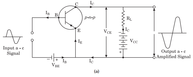
Question
Describe $p-n-p$ transistor as an amplifier in common emitter configuration with proper circuit diagram.

Answer

Common Emitter $p-n-p$ Transistor Amplifier : Circuit Diagram : For this amplifier the circuit diagram is shown in Fig. (a) in which emitter is made common to input and output circuits.
Action : Here the input circuit is forward biased by a low voltage battery $V _{ BE }$ and the output circuit is reversed biased by a high voltage battery Vcc. Thus, the resistance of the input (≈ 1 ΚΩ) is low and that of output is high (= 50 ΚΩ).
Image
A load resistance RL is connected in collector-emitter circuit i.e., output circuit. The weak input a.c signal is applied in the base-emitter circuit and the amplified output a.c. signal is obtained across RL in the collector emitter circuit i.e., output circuit.
When there is no a.c. input voltage signal in the circuit then according to Kirchhoff's current law, the relation between emitter current IE base current IB and collector current IC will be :
$I_E=I_B+I_C$ ...(1)
where IC is sightly less than IE due to a bit small value of IB.
Now due to collector current IC the potential drop across the load resistance RL will be, IC RL Therefore, the potential difference between collector and emitter i.e., collector-emitter voltage VCE would be given by
$V_{C E}=V_{C C}-I_C \cdot R_L$ ...(2)
But when the a.c. input voltage signal (which is to be amplified) is applied in the input circuit, it changes the base-emitter voltage VBE due to which emitter current IE and correspondingly the collector current IC will be changed. The change in the base current IB being very small.
Thus, due to change in IC according to equation (2), the voltage VCE varies. This variation in VCE due to input a.c. signal appears as an amplified output across the load resistance RL.
Phase Relationship between Input and Output Voltage Signals : In first positive half-cycle of a.c. input it opposes the forward biasing of input circuit resulting in reduction in forward biasing of this base-emitter circuit. Due to this the emitter current $I _{ E }$ decreases and correspondingly there is a decrease in collector current $I _{ C }$ also. Hence according to the equation $V_{C E}=V_{C C}-I_C R_L$, the decrease in $I _{ C }$ results in an increase in voltage VCE . Since collector is connected to the negative terminal of the biasing battery VCC hence an increase in voltage $V _{ CE }$ means that it becomes more negative.
This in first positive half-cycle amplified amplitude of the output signal in negative direction is obtained.
In the next negative half-cycle of the input signal it supports the forward biasing of the base-emitter circuit. Therefore, the emitter current IE and correspondingly the collector current IC both increases. As a result on the bases of equation $V_{C E}=V_{C C}-I_C \cdot R_L$, the voltage VCE decreases, hence the collector becomes less negative. In this way in the next negative half-cycle amplified amplitude of the output signal in the positive direction is obtained.
Hence it may be conclude that in common-emitter transistor amplifier the output voltage signal is in opposite phase to that of input signal i.e., output voltage signal is 180° out of phase with the input voltage signal.
Constants of Common Emitter Transistor Amplifier:
The various constants i.e., gains of a common emitter transistor amplifier are defined as follows which are similar for both types i.e., $p-n-p$ and $n-p-n$ transistor amplifiers.
(i) A.C. Current Gain i.e., Current Amplification Factor : "It is defined as the ratio of the change in the collector current to the change in the base current when collector-emitter voltage is kept constant." It is denoted by $\beta_{a c}$
$\therefore \quad \beta_{a c}=\left(\frac{\Delta I _{ C }}{\Delta I _{ B }}\right)_{ V _{ C E } \text { constant }}$ ...(1)
The value of $\beta$ is from 15 to 50 .
(ii) A.C. Voltage Gain i.e., Voltage Amplification Factor : "It is defined as the ratio of the change in the output voltage to the change in the input voltage." It is denoted by AV.
$\therefore \quad A _{ V }=\left(\frac{ V _o}{V_i}\right)$ ...(2)
But $V _o=\Delta I _{ C } \times R _o$ and $V _i=\Delta I _{ B } \times R _i$
Where $R _o=$ Output resistance
And $R _i=$ Input resistance
$\Delta I _{ C }=$ Change in collector current
and $\Delta I _{ B }=$ Change in base current
$\therefore \quad A _{ V }=\frac{\Delta I _{ C } \times R _o}{\Delta I _{ B } \times R _i}=\left(\frac{\Delta I _{ C }}{\Delta I _{ B }}\right)\left(\frac{ R _o}{ R _i}\right)$
But $\frac{\Delta I _{ C }}{\Delta I _{ B }}=$ Current gain $\beta_{\text {a.c. }}$ and $\frac{ R _o}{ R _i}=$ Resistance gain
$\therefore \quad A_V=\beta_{a c} \times \text { resistance gain }$ ... (3)
Since $\beta_{ ac } \gg \alpha_{ ac }$ hence $A _{ V }$ for C.E amplifier is larger than that for CB amplifier.
(iii) A.C. Power Gain or Power Amplification Factor : "It is defined as the ratio of the change in output power to the change in input power. "It is denoted by Pac.
∵ Power, $P = I \times V$
$P _{ ac }=$ a.c. current gain × a.c. voltage gain
$P_{a c}=\beta_{a c} \times A_V$
$=\beta_{ ac } \times\left(\beta_{ ac } \times\right.$ resistance gain $)$
$\Rightarrow \quad P _{ ac }=\beta_{ ac }^2 \times$ resistance gain ...(4)

Need a full question paper?

Generate a complete, print-ready paper with questions like this in minutes — across 16+ boards, with answer keys.

Start Generating Free

Similar questions

In an experiment on photoelectric effect, the emitter and the collector plates are placed et a separation of 10cm and are connected through en ammeter without any cell A magnetic field B exists parallel to the plates. The work function of the emitter is 2.39eV and the light incident on it has wavelengths between 400nm and 600nm. Find the minimum value of B for which the current registered by the ammeter is zero. Neglect any effect of space charge.
It is required to construct a $10\mu\text{F}$ capacitor which can be connected across a 200V battery. Capacitors of capacitance $10\mu\text{F}$ are available but they can withstand only 50V. Design a combination which can yield the desired result.
Calculate the:
  1. Momentum and,
  2. De Broglie wavelength of the electrons accelerated through a potential difference of $56 V.$
A given coin has a mass of 3.0 g. Calculate the nuclear energy that would be required to separate all the neutrons and protons from each other. For simplicity assume that the coin is made entirely of ${ }_{29}^{63} Cu$ atoms (of mass 62.92960 u).
Electric field in the given figure is directed along $+X$ direction and given by $Ex = 5A_x + 2B,$ where $E$ is in $NC^{-1}$ and $x$ is in metre$, A$ and $B$ are constants with dimensions. Taking $A = 10\ NC^{-1} m^{-1}$ and $B = 5\ NC^{-1},$ calculate:
  1. The electric flux through the cube.
  1. Net charge enclosed within the cube.
Answer the following question:
Long distance radio broadcasts use short-wave bands. Why?
Find the value of $\frac{\text{i}_1}{\text{i}_2}$ in the figure. if (a) $\text{R}=0.1\Omega$ (b) $\text{R}=1\Omega$ and (c) $\text{R}=10\Omega.$ Note from your answers that in order to get more current from a combination of two batteries, they should be joined in parallel if the external resistance is small and in series if the external resistance is large, compared to the internal resistance.
Ultraviolet light of wavelength $2271 \mathring A$ from a $100 W$ mercury source irradiates a photo $-$ cell made of molybdenum metal. If the stopping potential is $–1.3 V,$ estimate the work function of the metal. How would the photo $-$ cell respond to a high intensity $(\sim 10^5 W m^2)$ red light of wavelength $6328 \mathring A$ produced by a He $-$ Ne laser?
Establish the formula for the capacitance of a parallel plate capacitor in the presence of dielectric material completely and partially.
A solenoid of length $20\ cm$, area of cross-section $4.0\ cm^2$ and having $4000$ turns is placed inside another solenoid of $2000$ turns having a cross$-$sectional area $8.0\ cm^2$ and length $10\ cm$. Find the mutual inductance between the solenoids.