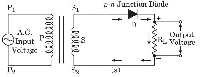
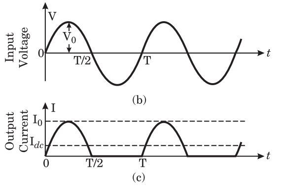
How is $p-n$ junction diode is used as an half wave rectifier? Explain its action with proper circuit diagram. Show the input and output waveform also.
How are fundamental logic gates OR, AND and NOT obtained from NOR gates ?
Answer
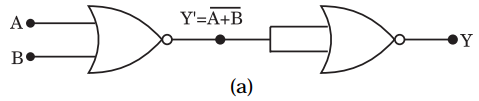
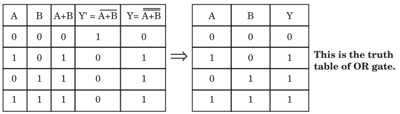
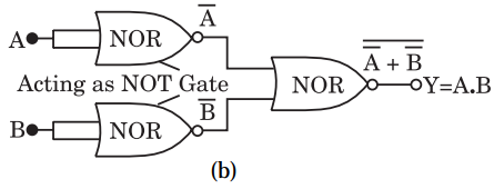
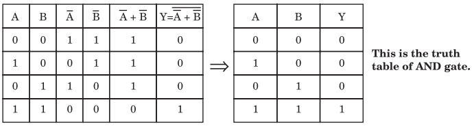
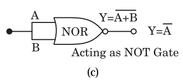
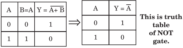
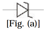
(1) To get OR Gate from NOR Gate : When output of a NOR gate is made input of a NOT gate obtained with the help of another NOR gate then OR gate is obtained. [Fig. (a)] Boolean Expression : $Y =\overline{\overline{ A \cdot B }}=\overline{\overline{ A } \cdot \overline{ B }}= A + B$ This can be explained with the help of truth table as follows : (2) To obtain AND gate from NOR gate : By using three NOR gates interconnected in the following manner as shown in figure (b), an AND gate can be obtained. Thus : $Y =\overline{\overline{ A } \cdot \overline{ B }} \Rightarrow Y = A \cdot B$ This can be explained with the help of truth table as follows : (3) To obtain NOT gate from NOR gate : By joining both the input terminals of a NOR gate, one input NOR gate is obtained which behaves as a NOT gate [Fig. (c)]. In NOR gate output is high when both the inputs are low and output is low when either or both the inputs are high. Here $Y =\overline{ A + B }$ or $Y =\overline{ A }($ i.e. $A = B )$ This can be explained with the help of truth table as follows :