Maharashtra BoardEnglish MediumSTD 12 SciencePhysicsQuestion Bank [ 2022 ]3 Marks
Question
Explain the working of the PNP transistor?
✓
Answer
Working of p-n-p transistor:
The majority of charge carriers in the emitter of the p-n-p transistor are holes.
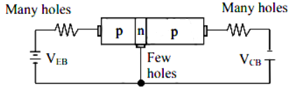
A typical biasing of a transistor is shown in figure (a). In this, the emitter-base junction is forward biased while the collector-base junction is reverse biased. Figure (a)
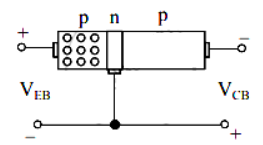
At the instant when the EB junction is forward biased, holes in the emitter region have not entered the base region as shown in figure (b). Figure (b)
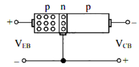
When the biasing voltage $V_{BE}$ is greater than the barrier potential $(0.6 – 0.7 V$ for Si transistors), many holes enter the base region and form the emitter current $I_E$ as shown in figure (c). Figure (c)
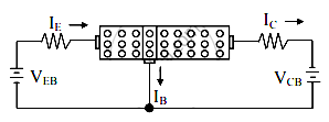
v. These holes can either flow through the base circuit and constitute the base current $\left( I _{ B }\right)$, or they can also flow through the collector circuit and contribute towards the collector current ( $I _{ C }$ ).
vi. The base is thin and lightly doped, the base current is only $5 \%$ of $I _{ E }$.
vii. Holes injected from the emitter into the base diffuse into the collector-base depletion region due to the thin base region. When the holes enter the collector-base depletion region, they are pushed into the collector region by the electric field at the collector-base depletion region. The collector current ( $l _{ C }$ ) flows through the external circuit as shown in figure (d). The collector's current $I _{ C }$ is about $95 \%$ of $I _{ E }$. Figure (d)
From the figure, we can conclude that $I_E = I_B + I_C$ Since the base current IB is very small we can write $I_C ≈ I_E.$
Need a full question paper?
Generate a complete, print-ready paper with questions like this in minutes — across 16+ boards, with answer keys.