For germanium crystal, the forbidden energy gap in joules is
[MP PET 2000]


Download our appand get started for free
Experience the future of education. Simply download our apps or reach out to us for more information. Let's shape the future of learning together!No signup needed.*
Similar Questions
- 1View SolutionThe amplification produced by a triode is due to the action of
- 2View SolutionIn a common base amplifier the phase difference between the input signal voltage and the output voltage is
- 3In a $P-N$ junction diode if $P$ region is heavily doped than $n$ region then the depletion layer isView Solution
- 4View SolutionThe phase difference between input and output voltages of a CE circuit is
- 5View SolutionThe temperature coefficient of resistance of a semiconductor
- 6Consider the following statements $A$ and $B$ and identify the correct choice of the given answers$A$ : The width of the depletion layer in a $P-N$ junction diode increases in forwards bias$B$ : In an intrinsic semiconductor the fermi energy level is exactly in the middle of the forbidden gapView Solution
- 7View SolutionThe electrical circuits used to get smooth d.c. output from a rectifier circuit is called
- 8View SolutionElectric current is due to drift of electrons in
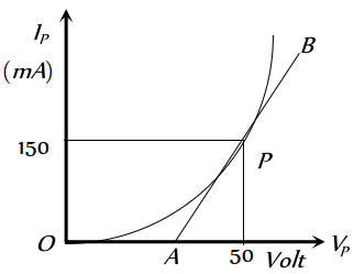
- 9The plate characteristic curve of a diode in space charge limited region is as shown in the figure. The slope of curve at point $P$ is $5.0 m A / V$. The static plate resistance of diode will beView Solution
- 10The curve between the work function of a metal $\left(\phi_o\right)$ and its temperature $(T)$ will beView Solution