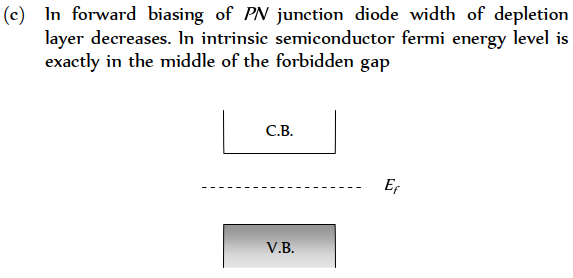
Consider the following statements $A$ and $B$ and identify the correct choice of the given answers$A$ : The width of the depletion layer in a $P-N$ junction diode increases in forwards bias$B$ : In an intrinsic semiconductor the fermi energy level is exactly in the middle of the forbidden gap
[EAMCET (Engg.) 2000]


Download our appand get started for free
Experience the future of education. Simply download our apps or reach out to us for more information. Let's shape the future of learning together!No signup needed.*
Similar Questions
- 1The depletion layer in silicon diode is $1 \mu m$ wide and the knee potential is $0.6 V$, then the electric field in the depletion layer will beView Solution
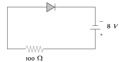
- 2A source voltage of $8 V$ drives the diode in fig. through a currentlimiting resistor of $100 ohm$. Then the magnitude of the slope load line on the $V-I$ characteristics of the diode isView Solution
- 3For a triode, at $V_g=-1$ volt, the following observations were taken $V_p=75 V , I_p=2 mA , V_p=100 V , I_p=4 mA$. The value of plate resistance will beView Solution
- 4View SolutionIn comparison to a half wave rectifier, the full wave rectifier gives lower
- 5In an amplifier the load resistance $R_L$ is equal to the plate resistance $\left(r_p\right)$. The voltage amplification is equal toView Solution
- 6Consider the following statements $A$ and $B$ and identify the correct choice of the given answers(A) A zener diode is always connected in reverse bias(B) The potential barrier of a $P N$ junction lies between $0.1$ to $0.3\ V$ approximatelyView Solution
- 7If $l_1, l_2, l_3$ are the lengths of the emitter, base and collector of a transistor thenView Solution
- 8Which impurity is doped in $S i$ to form $N$-type semi-conductor?View Solution
- 9A potential barrier of $0.50 \quad V$ exists across a $P-N$ junction. If the depletion region is $5.0 \times 10^{-7} m$ wide, the intensity of the electric field in this region isView Solution
- 10The curve between charge density and distance near $P-N$ junction will beView Solution