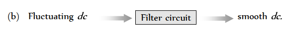
The electrical circuits used to get smooth d.c. output from a rectifier circuit is called
[KCET 2000]


Download our appand get started for free
Experience the future of education. Simply download our apps or reach out to us for more information. Let's shape the future of learning together!No signup needed.*
Similar Questions
- 1View SolutionIn a triode valve
- 2In the middle of the depletion layer of a reverse-biased $P N$ junction, theView Solution
- 3View SolutionIf the forward voltage in a semiconductor diode is doubled, the width of the depletion layer will
- 4Consider the following statements $A$ and $B$ and identify the correct choice of the given answers$A$ : The width of the depletion layer in a $P-N$ junction diode increases in forwards bias$B$ : In an intrinsic semiconductor the fermi energy level is exactly in the middle of the forbidden gapView Solution
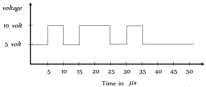
- 5View SolutionIn a negative logic the following wave form corresponds to the
- 6View SolutionIn intrinsic semiconductor at room temperature, number of electrons and holes are
- 7View SolutionIn a junction diode, the holes are due to
- 8In an NPN transistor circuit, the collector current is $10 mA$. If $90 \%$ of the electrons emitted reach the collector, the emitter current ( $i$ ) and base current $(i)$ are given byView Solution
- 9View SolutionThe emitter-base junction of a transistor is biased while the collector-base junction is biased
- 10View SolutionSymbolic representation of photodiode is