The forbidden energy band gap in conductors, semiconductors and insulators are $E G_1, E G_2$ and $E G_3$ respectively. The relation among them is
[MP PMT 1994; RPMT 1997]


Download our appand get started for free
Experience the future of education. Simply download our apps or reach out to us for more information. Let's shape the future of learning together!No signup needed.*
Similar Questions
- 1In a diode valve the cathode temperature must be ( $\phi=$ work function)View Solution
- 2To obtain a $P$-type germanium semiconductor, it must be doped withView Solution
- 3View SolutionHoles are charge carriers in
- 4In NPN transistor the collector current is $10\ mA$. If $90 \%$ of electrons emitted reach the collector, thenView Solution
- 5In a transistor, a change of $8.0 mA$ in the emitter current produces a change of $7.8 mA$ in the collector current. What change in the base current is necessary to produce the same change in the collector currentView Solution
- 6In a transistor circuit shown here the base current is $35 \mu A$. The value of the resistor $R$ isView Solution
- 7If $\alpha=0.98$ and current through emitter $i=20\ mA$, the value of $\beta$ isView Solution
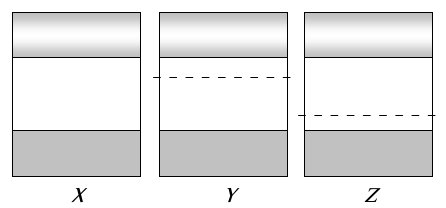
- 8View SolutionThe energy band diagrams for three semiconductor samples of silicon are as shown. We can then assert that
- 9View SolutionIn P-type semiconductor, there is
- 10View SolutionGaAs is