When a $P N$ junction diode is reverse biased


Download our appand get started for free
Experience the future of education. Simply download our apps or reach out to us for more information. Let's shape the future of learning together!No signup needed.*
Similar Questions
- 1View SolutionThe valence band and conduction band of a solid overlap at low temperature, the solid may be
- 2View SolutionFor non-conductors, the energy gap is
- 3Barrier potential of a $P-N$ junction diode does not depend onView Solution
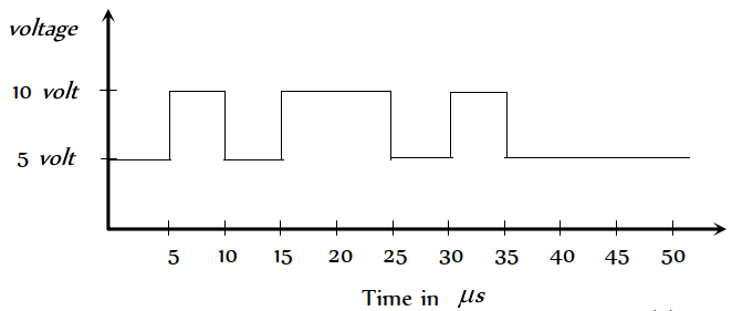
- 4View SolutionIn a negative logic the following wave form corresponds to the
- 5If the amplification factor of a triode $(\mu)$ is 22 and its plate resistance is $6600 ohm$, then the mutual conductance of this valve is mho isView Solution
- 6$N$-type semiconductors will be obtained, when germanium is doped withView Solution
- 7While a collector to emitter voltage is constant in a transistor, the collector current changes by $8.2 mA$ when the emitter current changes by $8.3 mA$. The value of forward current ratio $h$ isView Solution
- 8View SolutionIn a common base amplifier the phase difference between the input signal voltage and the output voltage is
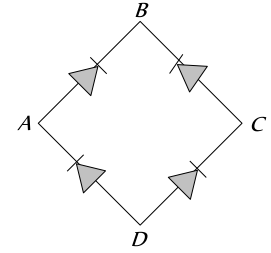
- 9In the diagram, the input is across the terminals $A$ and $C$ and the output is across the terminals $B$ and $D$, then the output isView Solution
- 10View SolutionSemiconductor is damaged by the strong current due to