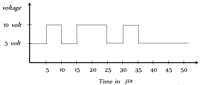
In a negative logic the following wave form corresponds to the


Download our appand get started for free
Experience the future of education. Simply download our apps or reach out to us for more information. Let's shape the future of learning together!No signup needed.*
Similar Questions
- 1Wires $P$ and $Q$ have the same resistance at ordinary (room) temperature. When heated, resistance of $P$ increases and that of $Q$ decreases. We conclude thatView Solution
- 2View SolutionThe voltage gain of a triode depends upon
- 3In $P$-type semiconductor the majority and minority charge carriers are respectivelyView Solution
- 4For a common base configuration of $P N P$ transistor $\frac{l_C}{l_E}=0.98$ then maximum current gain in common emitter configuration will beView Solution
- 5Consider the following statements $A$ and $B$ and identify the correct choice of the given answers$A$ : The width of the depletion layer in a $P-N$ junction diode increases in forwards bias$B$ : In an intrinsic semiconductor the fermi energy level is exactly in the middle of the forbidden gapView Solution
- 6The reason of current flow in $P-N$ junction in forward bias isView Solution
- 7View SolutionSymbolic representation of photodiode is
- 8$14 \times 10^{15}$ electrons reach the anode per second. If the power consumed is 448 milliwatts, then the plate (anode) voltage isView Solution
- 9In a common emitter transistor, the current gain is $80.$ What is the change in collector current, when the change in base current is $250 \mu A$View Solution
- 10In NPN transistor the collector current is $10\ mA$. If $90 \%$ of electrons emitted reach the collector, thenView Solution