When forward bias is applied to a $P-N$ junction, then what happens to the potential barrier $V_B$, and the width of charge depleted region $x$
[UPSEAT 2002, 03;Roorkee 1999; RPET 2003; AIEEE 2004]


Download our appand get started for free
Experience the future of education. Simply download our apps or reach out to us for more information. Let's shape the future of learning together!No signup needed.*
Similar Questions
- 1In a $P$-type semiconductor, germanium is doped withView Solution
- 2A semiconductor is cooled from $T_1 K$ to $T_2 K$. Its resistanceView Solution
- 3The slope of plate characteristic of a vacuum tube diode for certain operating point on the curve is $10^{-3} \frac{ mA }{ V }.$ The plate resistance of the diode and its nature respectivelyView Solution
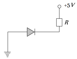
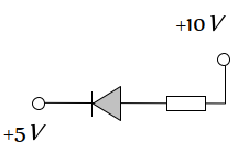
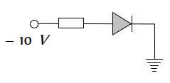
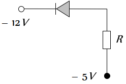
- 4View SolutionIn the given figure, which of the diodes are forward biased ?
- 5The reverse biasing in a $P N$ junction diodeView Solution
- 6View SolutionA pure semiconductor behaves slightly as a conductor at
- 7View SolutionIn comparison to a half wave rectifier, the full wave rectifier gives lower
- 8View SolutionIn a triode amplifier, the value of maximum gain is equal to
- 9Carbon, silicon and Germanium atoms have four valence electrons each. Their valence and conduction band are separated by energy band gaps represented by $(E) .(E)$ and $(E)$ respectively. Which one of the following relationship is true in their caseView Solution
- 10View SolutionWhen NPN transistor is used as an amplifier