When $G e$ crystals are doped with phosphorus atom, then it becomes
[AFMC 1995; Orissa PMT 2004]


Download our appand get started for free
Experience the future of education. Simply download our apps or reach out to us for more information. Let's shape the future of learning together!No signup needed.*
Similar Questions
- 1View SolutionSymbolic representation of photodiode is
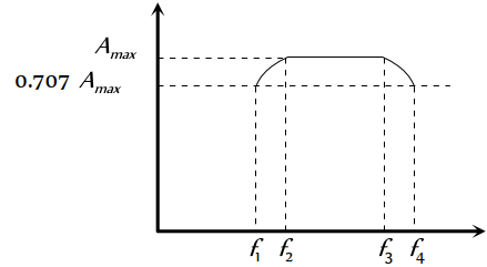
- 2The frequency response curve of $R C$ coupled amplifier is shown in figure. The band width of the amplifier will beView Solution
- 3For a transistor the parameter $\beta=99$. The value of the parameter $\alpha$ isView Solution
- 4View SolutionIn an insulator, the forbidden energy gap between the valence band and conduction band is of the order of
- 5View SolutionIn comparison to a half wave rectifier, the full wave rectifier gives lower
- 6View SolutionThe band gap in Germanium and silicon in eV respectively is
- 7View SolutionFor non-conductors, the energy gap is
- 8In the circuit of a triode valve, there is no change in the plate current, when the plate potential is increased from $200$ volt to $220$ volt and the grid potential is decreased from $-0.5$ volt to $-1.3$ volt. The amplification factor of this valve isView Solution
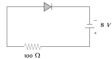
- 9A source voltage of $8 V$ drives the diode in fig. through a currentlimiting resistor of $100 ohm$. Then the magnitude of the slope load line on the $V-I$ characteristics of the diode isView Solution
- 10View SolutionGaAs is