The band gap in Germanium and silicon in eV respectively is


Download our appand get started for free
Experience the future of education. Simply download our apps or reach out to us for more information. Let's shape the future of learning together!No signup needed.*
Similar Questions
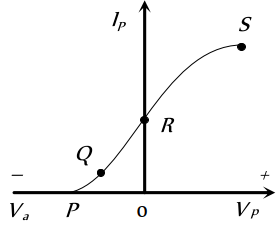
- 1View SolutionThe point representing the cut off grid voltage on the mutual characteristic of triode is
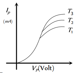
- 2View SolutionFor the diode, the characteristic curves are given at different temperature. The relation between the temperatures is
- 3View SolutionDue to S.C.R in vacuum tube
- 4Silicon is a semiconductor. If a small amount of $A s$ is added to it, then its electrical conductivityView Solution
- 5In a full wave rectifiers, input $a c$ current has a frequency ' $v$. The output frequency of current isView Solution
- 6In extrinsic $P$ and $N$-type, semiconductor materials, the ratio of the impurity atoms to the pure semiconductor atoms is aboutView Solution
- 7Electronic configuration of germanium is $2,8,18$ and $4$ . To make it extrinsic semiconductor small quantity of antimony is addedView Solution
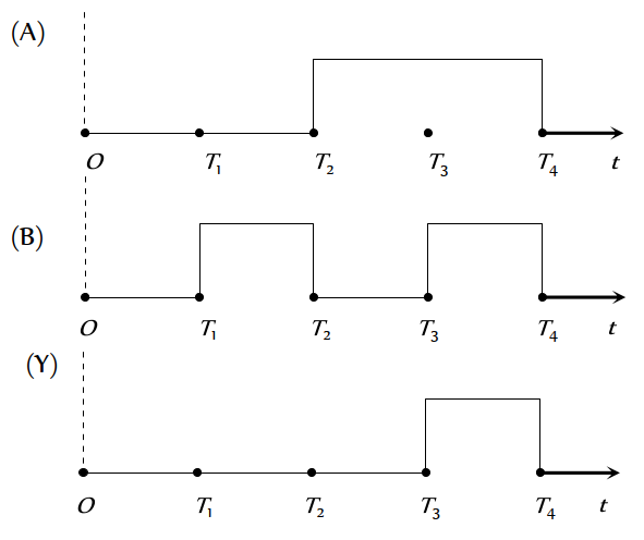
- 8The given figure shows the wave forms for two inputs $A$ and $B$ and that for the output $Y$ of a logic circuit. The logic circuit isView Solution
- 9View SolutionWhich one of the following statements is not correct
- 10The forbidden energy band gap in conductors, semiconductors and insulators are $E G_1, E G_2$ and $E G_3$ respectively. The relation among them isView Solution