MCQ 11 Mark
The accepter impurity in following is -
- AArsenic
- BPhosphorus
- ✓Indium
- DAntimony
Answer
View full question & answer→Correct option: C.
Indium
C
50 questions · timed · auto-graded
Explanation:
The junction voltage Vo for a germanium diode is 0.3 V at room temperature. This potential opposes the diffusion of electrons from n-side and holes from p-side. It is 0.7 eV for Si at room temperature.
Explanation:
In n-type semiconductor, large number of free electrons is present. Hence, free electrons are the majority charge carriers in the n-type semiconductor. The free electrons (majority charge carriers) carry most of the electric charge or electric current in the n-type semiconductor.
Explanation:
Insulators have large energy gap between valence and conduction band (about 6eV), while semiconductors have a smaller one and conductors, the smallest energy gap.
Explanation:
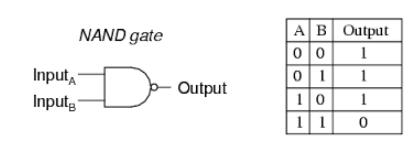
The truth table of NAND gate is shown as above, which implies that if at least one of the input is low then the output is high.
Explanation:
The zener voltage will be a constant only when it is operating in the breakdown region.
Explanation:
Because of the difference in the concentration of charge carriers in the p−n junction, holes from the p side move to the n side and electrons from the n side move to the p side. This motion of charge carriers gives rise to diffusion current.
Because of this, a negative space charge region is formed in the p region and a positive space region is formed in the n region. This sets up an electric field across the junction. Thus, there is a constant electric field near the junction.
This electric field further opposes the diffusion of majority charge carriers across the junction. As a result, an electron from the p region starts moving to the n region and a hole from the n region starts moving to the p region. This sets up drift current. Thus, there is a systematic flow of charge carriers across the junction. Also, there is no net charge transfer between the two sides.
Explanation:
A voltage regulator circuit can be designed using a zener diode to maintain a constant DC output voltage across the load in spite of variations in the input voltage or changes in the load current.
Explanation:
A NOT gate inverts the input signal which is the same as complementing a signal or changing the logic in a digital circuit. This means that when the input to the NOT gate is logic '0', the output is logic '1'. However, it does not stop a signal.
Explanation:
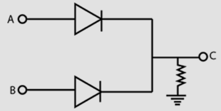
The image given shows a diode OR circuit. R is connected from the output to ground to provide bias current for the diodes. Any positive voltage will represent a logic 1 state and the summing of currents through multiple diodes does not change the logic level.
Explanation:
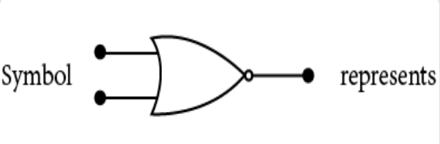
The symbol of circle shown in figure with OR gate indicates the NOT gate hence, given gate is NOR gate.
Explanation:
In an intrinsic semiconductor, the number density of electrons is equal to the number density of holes i.e ne = nh.
Since there is no doping, no extra hole or electron is produced.
Explanation:
In a p‒n junction, current flows only if it is connected to the battery. If two ends of a p‒n junction are joined by a wire, then there will be diffusion and drift currents in the circuit and they will cancel each other. Hence, no current will flow in the circuit.
Explanation:
A p-type semiconductor is produced by doping a 14 group element with a 13 group element as 14 group element has 4 valence electron whereas that of group 13 has 3 valence electron. We know that Germanium is a 14 group element and gallium is a 13 group element, thus doping germanium with gallium forms a p-type semiconductor.
Explanation:
In insulators, the electrons are tightly bound with the nucleus hence, at room temperature thermal energy is not enough to push the electrons into conduction band and hence, no electrons are available for conduction.
The energy required for electron to escape out from orbit and to over come the energy gap is thus of the order of 6 eV, while for semiconductors and conductors it is (of the order of) 1 eV and 0 respectively.
Explanation:
Optoelectronic devices and components are those electronic devices that operate on both light and electrical currents. This can include electrically driven light sources such as laser diodes and light-emitting diodes, components for converting light to an electrical current such as solar and photovoltaic cells and devices that can electronically control the propagation of light.
Explanation:
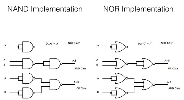
Truth table of NOR is complement of OR. That's why NOR is combination of OR gate followed by NOT gate.
Explanation:
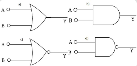
a- represent OR gate
b- represent the AND gate
c- represent, the combination of OR and NOT gate, NOR gate.
d- represent, the combination of AND and NOT gate, NAND gate.
Explanation:
The process by which ac is converted into dc is known as "Rectification".
Statement-2: NOT gate inverts the input order.
Explanation:
NOT gate is also called invertor circuit since NOT gate inverts the input order. Hence, statement 1-is true statement-2 is true statement-2 is correct explanation of statement-1.
Explanation:
When Zener diode is connected in reverse bias, as applied voltage reaches at Zener breakdown voltage, due to rupture of bonds there is a sudden increase in current in Zener diode.
Explanation:
In an intrinsic semiconductor, n=p, where, n is number of electrons and p is number of holes in intrinsic semiconductor.
This implies that there is an equal chance of finding an electron at the conduction band edge as there is of finding a hole at the valence band edge. Thus, the average energy level of electrons and holes is half of the energy band gap in intrinsic semiconductors.
Also the Fermi energy level lie exactly in the middle of energy band gap in intrinsic semiconductors. Thus, the value indicated by Fermi energy level in an intrinsic semiconductor is the average energy of electrons and holes.
Explanation:
In reverse bias, 'p' region of a semi conductor is connected to negative pole and 'n' region to positive pole.
Explanation:
NAND and NOR gates are known as universal gates. Any one of these gates can be used to implement any kind of logic gate. This kind of feasibility is does not exist with other gates i.e. any other gate cannot solely implement all logic gates. For example, AND gate cannot be implemented using an OR gate and vice-versa. The implementation of NAND and NOR gates to generate other logic gates is shown above.
Explanation:
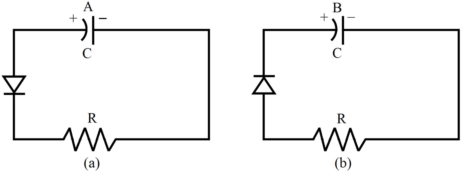
In circuit (a), the diode is forward biassed. So, it offers negligible resistance to the flow of current and can thus be replaced by a short circuit. Now, the capacitor charge will leak through the resistance and decay exponentially with time.
Capacitor charge $=\frac{\text{VC}}{\text{e}}$
In circuit (b), the diode is reverse biassed. So, it offers infinite resistance to the current flow and can thus be replaced by an open circuit. As the circuit is open now, no current can flow across the resistance. So, the charge in the capacitor cannot leak through the resistor.
Capacitor charge = VC
Explanation:
When a p‒n junction is formed then because of the difference in the concentration of charge carriers in the two regions, electrons from the n region move to the p region and holes from the p region move to the n region. Since the direction of the current is always opposite to the motion of electron, the direction of the current is from the p side to the n side.
Similarly, when the junction is forward biassed, the positive terminal of the battery is connected to the pside of the p‒n junction and the negative terminal of the battery is connected to the n side of the p‒njunction. As a result, electrons in the n side of the p‒n junction are repelled by the negative terminal of the battery and they move to the p side, where the positive terminal of the battery attracts them. Similarly, holes from the p side of the p‒n junction are repelled by the positive terminal of the battery and they move to the n side, where the negative terminal of the battery attracts them. Thus, they give diffusion current from the p side to the n side across the p‒n junction.
In reverse biassing, there is no flow of majority carriers across the junction; hence, there is not diffusion current. Here, the flow of majority carriers is opposed by the applied voltage.
Explanation:
Semiconductors in their natural state are poor conductors because a current requires the flow of electrons, and semiconductors have their valence band filled, preventing the entry flow of new electrons.
Thus semi-conductors allows a large current to pass through them.
Explanation:
A p-type semiconductor is formed by doping a pure semiconductor with a p-type material. As impurity atoms take the position of the germanium atom in a germanium crystal, three electrons of a p-type material form covalent bonds by sharing electrons with three neighbouring germanium atoms. However, the fourth covalent bond is left incomplete, with a want of one electron. This creates a hole. As the atom as a whole is neutral, the p-type material is also neutral.
Explanation:
We know that the conductivity of any semiconductor can be increased by increasing the number of charge carriers. All the given methods are effective in increasing the number of free charge carriers. Hence, all options are correct.
Explanation:
A hole diffuses from the p side to the n side in a p−n junction; that is, an electron moves from the n side to the p side. This implies that a bond is broken on the n side. As the electron travels towards the p side, which is rich in holes, it combines with a hole. A hole is created because of the deficiency of one electron. So, when an electron combines with a hole, it completes that bond.
Explanation:
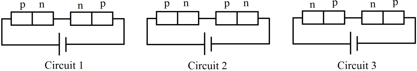
In circuit 1, one diode is forward biassed and the other diode is reverse biassed. The forward-biassed diode offers zero resistance (ideally) to the current flow, so it can be replaced by a short circuit. The voltage drop across the first diode will be zero. The second diode is reverse biassed, so it can be replaced by an open circuit; hence, the voltage drop across this diode will be maximum.
In circuit 2, both the diodes are forward biassed, so they can be replaced by short circuits; hence, the voltage drop across both of them will be minimum and equal.
In circuit 3, both the diodes are reverse biassed, so both can be replaced by open circuits; hence, the voltage drop across both of them will be maximum and equal.
There are no free electrons at 0K.
The number of free electrons increases with temperature.
The number of free electrons is less than that in a conductor.
Explanation:
In semiconductors, the valence band is full at 0K, but the conduction band is empty. So, no free electron is available for conduction at 0K.
As the temperature increases, covalent bonds that provide free charge carriers for conduction in a semiconductor break.
As the conduction band in metals is already partially filled at 0K, many free electrons below the Fermi level acquire energy from an external source or temperature, jump to the conduction band and start behaving like free electrons. Hence, metals contain more free electrons than semiconductors.
Explanation:
After the diffusion of majority charge carriers across a p‒n junction, an electric field is set up because of the accumulation of immobile ions at the junction. These further oppose the motion of majority charge carriers across the junction. As a result, electrons from the p region start moving to the n region and holes from the n region start moving to the p region. This constitutes the drift current. As the direction of the current is opposite to the direction of the motion of the electrons, the direction of the drift current is from the n side to the p side.
In forward biasing, there is no movement of electrons from the p region to the n region and of holes from the n region to the p region. Hence, there is not drift current.
Explanation:
In the forward biassing of a p−n junction, the positive terminal of the battery is connected to the p side of the p−n junction and the negative terminal of the battery is connected to the n side of the p−n junction. As a result, electrons in the n side of the p−n junction are repelled by the negative terminal of the battery and move to the p side, where the positive terminal of the battery attracts the electrons. Similarly, holes from the p side of the p−n junction are repelled by the positive terminal of the battery and move to the nside, where the negative terminal of the battery attracts the holes. Thus, they give diffusion current across the p−n junction.
In case of reverse biassing, no conduction takes place across the junction because of the diffusion of majority carriers. Hence, there is no diffusion current.
If the junction is unbiased, then diffusion current is initially maximum. But at equilibrium, diffusion current becomes equal to drift current.
Explanation:
In a p‒n junction diode, diffusion current flows because of the diffusion of holes from the p side to the n side and of electrons from the n side to the p side. The current flowing in the diode due to the diffusion of charge carriers across the junction is called the diffusion current. The current flowing in the diode due to the movement of minority carriers across the junction due to their thermal energy is called the drift current. In an unbiased diode, the net current flowing across the junction is zero due to the cancellation of the drift current by the diffusion current. For the flow of diffusion and drift currents, holes and electrons are produced continuously throughout the material. When a hole crosses the junction, it combines with an electron on the n side. As the depletion region is devoid of free charge carriers, this recombination never takes place inside the depletion region.
Explanation:
As the intrinsic semiconductor is free from all impurities, the number of electrons is equal to the number of holes.
Explanation:
As a p−n junction allows the flow of current in forward bias and stops the current in reverse bias (almost negligible reverse leakage current flows in the reverse-biassed p−njunction), the device should be a p−n junction. Other options are examples of semiconductors that allow moderate current to flow and that do not have any effect of changing the polarity of the battery.