Questions · Page 2 of 5

M.C.Q [1M]

MCQ 511 Mark
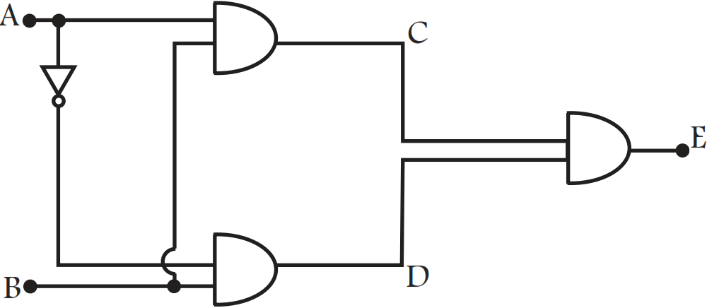
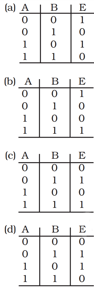
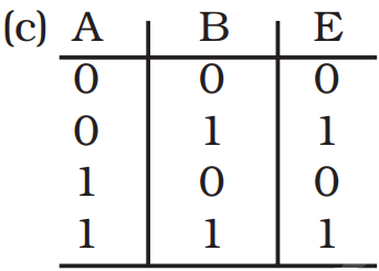
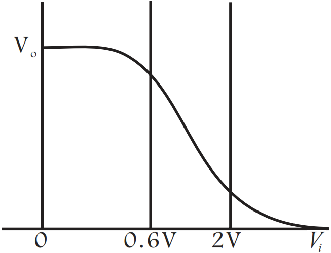
Figure shows the transfer characteristics of a base biased CE transistor. Which of the following statements are true?

  • A
    At Vi = 0.4V, transistor is in active state.
  • B
    At Vi = 1V, it can be used as an amplifier.
  • C
    At Vi = 0.5V, it can be used as a switch turned off.
  • D
    At Vi = 2.5V, it can be used as a switch turned on.
Answer
  1. At Vi = 1V , it can be used as an amplifier.
  2. At Vi = 0.5V, it can be used as a switch turned off.
  3. At Vi = 2.5V, it can be used as a switch turned on.

Solution:

According to above graph transfer characteristics of a base biased common emitter transistor, we note that.

  1. When Vi= 0.4 V, output voltage remain same,there is no collection current. So, transistor circuit is not in active state.
  2. when Vi = 1V (This is in between 0.6V to 2V), the transistor circuit is in active state and when input is increasing output is decreasing because when CE is used as an amplifier input and output voltages are 180º out of phase. Then it is used as an amplifier.
  3. when Vi = 0.5V, there is no collector current. The transistor is in cut off state. The transistor circuit can be used as a switch to be turned off.
  4. when Vi = 2.5V, the collector current becomes maximum and transistor is in a saturation state and can used as switch turned on state.
View full question & answer
MCQ 521 Mark
When npn transistor is used as an amplifier:
  • A
    Electrons move from collector to base.
  • B
    Holes move from emitter to base.
  • C
    Electrons move from base to collector.
  • D
    Holes move from base to emitter.
Answer
  1. Holes move from base to emitter.
View full question & answer
Question 531 Mark
Truth table for the given circuit (Fig.) is:

Answer

Solution:

Here, C = A.B and D = Ā.B

E = C + D = (A B) + (Ā .B)

Explanation The truth table of this arrangement of gates can be given 

A B Ā C = A.B d = Ā.B E = (C + D)
0 0 1 0 0 0
0 1 1 0 1 1
1 0 0 0 0 0
1 1 0 1 0 0
View full question & answer
MCQ 541 Mark
Electric conduction in a semiconductor takes place due to:
  • A
    Electrons only.
  • B
    Holes only.
  • C
    Both electrons and holes.
  • D
    Neither electrons nor holes.
Answer
  1. Both electrons and holes.
View full question & answer
MCQ 551 Mark
In the depletion region of a pn junction, there is a shortage of:
  • A
    Acceptor ions
  • B
    Holes and electrons
  • C
    Donor ions
  • D
    None of these
Answer
  1. Holes and electrons

Explanation:

Depletion region of a p-n junction is formed due to the shortage of holes and electrons.

View full question & answer
MCQ 561 Mark
Conventional flow of current will always be from:
  • A
    p type → n type
  • B
    n type → p type
  • C
    n Type → n type
  • D
    None of these
Answer
  1. p type → n type

Explanation:

The holes in the covalent bonds of p-type semiconductor. They appear to move towards n-type semiconductor. Because the electrons in the covalent bonds of n-type semiconductor (not free electrons) jump towards p-type semiconductor due to plenty of holes available in the covalent bonds at p-side. 

Hence, conventional current flow from p-type to n-type.

View full question & answer
MCQ 571 Mark
A transistor has three impurity regions. All the three regions have different doping levels. In order of increasing doping level, the regions are:
  • A
    Emitter, base and collector.
  • B
    Collector, base and emitter.
  • C
    Base, emitter and collector.
  • D
    Base, collector and emitter.
Answer
  1. Base, collector and emitter.
View full question & answer
MCQ 581 Mark
By increasing the temperature, the specific resistance of a conductor and a semiconductor:
  • A
    Increases for both.
  • B
    Decreases for both.
  • C
    Increases, decreases.
  • D
    Decreases, increases.
Answer
  1. Increases, decreases.
View full question & answer
MCQ 591 Mark
When an input signal 1 is applied to a NOT gate, its output is:
  • A
    1
  • B
    0
  • C
    either 0 or 1
  • D
    both 0 and 1
Answer
  1. 0

Explanation:

NOT gate yields the reverse of the input signal in output, thus when an input signal 1 is applied to a NOT gate, its output is 0.

View full question & answer
MCQ 601 Mark
The impurity atoms with which pure silicon may be doped to make it a p-type semiconductor are those of:
  • A
    Phosphorus.
  • B
    Boron.
  • C
    Antimony.
  • D
    Aluminium.
Answer
  1. Boron.

  1. Aluminium.

Explanation:

A p-type semiconductor is formed by doping an intrinsic semiconductor with a trivalent atom (atom having valency 3). As phosphorous and boron have three valence electrons, they can be doped with silicon to make a p-type semiconductor.

View full question & answer
MCQ 611 Mark
The free electron density is more in .....:
  • A
    Conductors
  • B
    Insulators
  • C
    Semi conductors
  • D
    Electrolytes
Answer
  1. Conductors

Explanation:

Free electron density is more in conductors that is why they are useful in conducting electricity.

View full question & answer
MCQ 621 Mark
Number of electrons in the valence shell of a semiconductor is:
  • A
    1
  • B
    2
  • C
    3
  • D
    4
Answer
  1. 4

Explanation:

The valency of semiconductor (Ge or Si) is four, hence it has 4 valence electrons in the outermost orbit of the Ge or Si-atom

View full question & answer
MCQ 631 Mark
In a PN junction:
  • A
    High potential at N side and low potential at P side.
  • B
    High potential at P side and low potential at N side.
  • C
    P and N both are at same potential.
  • D
    Undetermined.
Answer
  1. High potential at N side and low potential at P side.

Explanation:

View full question & answer
MCQ 641 Mark
A hole is:
  • A
    A positively charged electron.
  • B
    An electron in the valence band.
  • C
    An unfilled covalent bond.
  • D
    An excess electron in covalent bond.
Answer
  1. An unfilled covalent bond.

Explanation:

When the covalent bond breaks, electrons are freed from atom. The departure of electron from valence band creates vacancy in bond, this vacancy is known as hole. Hence, a hole is an unfilled covalent bond.

View full question & answer
MCQ 651 Mark
What is the order of magnitude of the resistance of a dry human body?
  • A
    10Ω
  • B
    104Ω
  • C
    10 MΩ
  • D
    10μΩ
Answer
  1. 104Ω

Explanation:

It is known that the resistance of a dry human body is 10kΩ = 104Ω.

View full question & answer
MCQ 661 Mark
The creation of voltage or electric current in a material upon exposure to light is termed as:
  • A
    Photo-ionic effect
  • B
    Thermi-ionic effect
  • C
    Photo-voltaic effect
  • D
    None of these.
Answer
  1. Photo-voltaic effect

Explanation:

The generation of current or voltage in a material, when exposed to light is called photovoltaic effect.
The device which operates on this effect is called photo-voltaic device or solar cell. It is a p-n junction diode which converts solar energy into electrical energy.

View full question & answer
MCQ 671 Mark
The leakage current across a pn junction is due to _________:
  • A
    Minority carriers
  • B
    Majority carriers
  • C
    Junction capacitance
  • D
    None of these
Answer
  1. Minority carriers

Explanation:

When a diode is reverse biased, its depletion region increases in width. Thus depletion region would correspond to an insulator. However still some current actually flows through the depletion region. This is due to the pushing of minority carriers across the depletion region causing very small reverse 'leakage current'.

View full question & answer
MCQ 691 Mark
Which of the following is/are optoelectronic devices?
  • A
    Photodiodes
  • B
    Solar cells
  • C
    Light emitting diodes
  • D
    All of the above
Answer
  1. All of the above

Explanation:

P-n junctions are an integral part of several optoelectronic devices. These include photodiodes, solar cells light emitting diodes (LEDs) and semiconductor lasers.

View full question & answer
MCQ 701 Mark
Two important processes that occur during the formation of a p-n junction.
  • A
    Diffusion
  • B
    Drift
  • C
    Both drift and diffusion
  • D
    Drift in p region and diffusion in n region
Answer
  1. Both drift and diffusion

Explanation:

Three important phenomena occurs during formation of pn junction:

Diffusion, Formation of space charge, Drift.

View full question & answer
MCQ 711 Mark
Filter circuit:
  • A
    Eliminates a.c. component.
  • B
    Eliminates d.c. component.
  • C
    Does not eliminate a.c. component.
  • D
    None of these.
Answer
  1. Eliminates a.c. component.
View full question & answer
MCQ 721 Mark
When an impurity is doped into semiconductor, the conductivity of the semiconductor:
  • A
    Increases
  • B
    Dcreases
  • C
    Remains same
  • D
    Becomes zero
Answer
  1. Increases

Explanation:

The pure semiconductor has less number of thermally generated charge carriers. But when it is doped with pentavalent or trivalent impurity atoms, the number of charge carriers i.e. electrons and holes increases. So conductivity increases.

View full question & answer
MCQ 731 Mark
Forward biasing is that in which applied voltage:
  • A
    Increases potential barrier.
  • B
    Cancels the potential barrier.
  • C
    Is equal to 1.5volt.
  • D
    None of these.
Answer
  1. Cancels the potential barrier.
View full question & answer
MCQ 741 Mark
Which of the following logic gates is an universal gate?
  • A
    OR
  • B
    NOT
  • C
    AND
  • D
    NOR
Answer
  1. NOR

Explanation:

NAND gate is considered universal gate. As other gates can be formed from this gate.

View full question & answer
MCQ 751 Mark
The current gain of a transistor in common base mode is 0.995. The current gain of the same transistor in common emitter mode is?
  • A
    197
  • B
    201
  • C
    198
  • D
    199
Answer
  1. 199
View full question & answer
MCQ 761 Mark
The lead marked with the arrow is the _______.

  • A
    collector
  • B
    base
  • C
    emitter
  • D
    core
Answer
  1. emitter

Explanation:

 It is a p-n-p, transistor. The Lead marked with the arrow is the emitter. It tells the direction of the flow of the holes i.e, the flow of conventional current. 

View full question & answer
MCQ 771 Mark
The following truth table is for: ABY 110 101 011 001
  • A
    NAND gate
  • B
    AND gate
  • C
    XOR gate
  • D
    NOT gate
Answer
  1. NAND gate

Explanation:

The output is 0 only when the two inputs are 1.

The output is 1 when any of the input is zero. 

This is the characteristic of a NAND gate.

View full question & answer
MCQ 781 Mark
Temperature coefficient of resistance of semiconductor is:
  • A
    Zero.
  • B
    Constant.
  • C
    Positive.
  • D
    Negative.
Answer
  1. Negative.
View full question & answer
MCQ 791 Mark
In the depletion region of a diode:
  • A
    There are no mobile charges.
  • B
    Equal number of holes and electrons exist, making the region neutral.
  • C
    Recombination of holes and electrons has taken place.
  • D
    Immobile charged ions exist.
Answer
  1. There are no mobile charges.
  2. Equal number of holes and electrons exist, making the region neutral.
  1. Immobile charged ions exist.

Solution:

On account of difference in concentration of charge carrier in the two sections of P-N junction, the electrons from N-rcgion diffuse through the junction into P-region and the hole from P-region diffuse into N-region.

​​​​​​​

Due to diffusion, neutrality of both N-and P-type semiconductor is disturbed, a layer of negative charged ions appear near the junction in the P-crystal and a layer of positive ions appears near the junction in N-crystal. This layer is called depletion layer.

The thickness of depletion layer is 1 micron = 10-6m.

Width of depletion layer ∞ 1/Dopping

Depletion is directly proportional to temperature.

Important point: The P-N junction diode is equivalent to capacitor in which the depletion layer acts as a dielectric.

View full question & answer
MCQ 801 Mark
When an electric field is applied across a semiconductor:
  • A
    Electrons move from lower energy level to higher energy level in the conduction band.
  • B
    Electrons move from higher energy level to lower energy level in the conduction band.
  • C
    Holes in the valence band move from higher energy level to lower energy level.
  • D
    Holes in the valence band move from lower energy level to higher energy level.
Answer
  1. Electrons move from lower energy level to higher energy level in the conduction band.
  1. Holes in the valence band move from higher energy level to lower energy level.

Solution:

As we apply electric field is applied across a semiconductor, the electrons in the conduction band acquire energy and get accelerated. They travel from lower energy level to higher energy level. While the holes in valence band travel from higher energy level to lower energy level, where they will be having more energy.

View full question & answer
MCQ 811 Mark
Carbon, silicon and germanium have four valence electrons each. At room temperature the appropriate statement is:
  • A
    The number of free electrons for conduction is significant only in Si and Ge but small in C.
  • B
    The number of free conduction electrons is significant in C but small Si and Ge.
  • C
    The number of free conduction electrons is negligibly small in all the three.
  • D
    The number of free conduction electrons is significant in all the three.
Answer
  1. The number of free electrons for conduction is significant only in Si and Ge but small in C.

Explanation:

In Si and Ge at room temperature(300K); the energy band gap is low as the result of which electrons in the covalent bonds gain kinetic energy, they break the bond and move to conduction band.

A hole is also created in the valence band. So the number of free electrons for conduction is significant in Si and Ge.

The energy band gap in case of carbon is high as the result of which there are not significant number of electrons in the conduction band even at room temperature.

View full question & answer
MCQ 821 Mark
Which of the following contains a covalent bond?
  • A
    Copper
  • B
    NaCl
  • C
    Germanium
  • D
    Helium
Answer
  1. Germanium

Explanation:

A covalent bond is a chemical bond that involves the sharing of electron pairs between atoms. The stable balance of attractive and repulsive forces between atoms when they share electrons is known as covalent bonding.

As the valency of germanium is 4, it can share 4 electrons of neighboring atom to complete the octet.

Hence, Ge has covalent bond. NaCl is an example of an ionic bond and helium and copper both have valency 2 and 1 respectively.

View full question & answer
MCQ 831 Mark
The pn junction can be formed by which of the following methods?
  • A
    Grown junction method
  • B
    Alloying method
  • C
    Diffusion method
  • D
    All of these
Answer
  1. All of these

Explanation:

Grown Junction Diode:

Diodes of this type are formed during the crystal pulling process. P and N-type impurities can be alternately added to the molten semiconductor material in the crucible, which results in a P-N junction when crystal is pulled. After slicing, the larger area device can then be cut into a large number of smaller-area semiconductor diodes. Though such diodes, because of larger area, are capable of handling large currents but larger area also introduces more capacitive effects, which are undesirable. Such diodes are used for low frequencies.

Alloy Type or Fused Junction Diode:

Such a diode is formed by first placing a P- type impurity (a tiny pellet of aluminium or some other P- type impurity) into the surface of an N-type crystal and heating the two until liquefaction occurs where the two materials meet. An alloy will result that on cooling will give a P-N junction at the boundary of the alloy substrate. Similarly, an N-type impurity may be placed into the surface of a P- type crystal and the two are heated until liquefaction occurs. Alloy type diodes have a high current rating and large PIV (peak inverse voltage) rating. The junction capacitance is also large, due to the large junction area.
View full question & answer
MCQ 841 Mark
In a npn transistor circuit, the collector current is 10mA. If 95 per cent of the electrons emitted reach the collector, which of the following statements are true?
  • A
    The emitter current will be 8mA.
  • B
    The emitter current will be 10.53mA.
  • C
    The base current will be 0.53mA.
  • D
    The base current will be 2mA.
Answer
  1. The emitter current will be 10.53mA.
  2. The base current will be 0.53mA.

Solution:

Given Ic = 10mA

According to the question, $\text{I}_\text{c}=\frac{95}{100}\text{I}_\text{e}$

$\Rightarrow\ \text{I}_\text{e}=\frac{10\times100}{95}=10.53\text{mA}$

We know that, Ib = Ie = Ic = 10.53 - 10 = 0.53mA.

View full question & answer
MCQ 851 Mark
A semiconductor is doped with a donor impurity:
  • A
    The hole concentration increases.
  • B
    The hole concentration decreases.
  • C
    The electron concentration increases.
  • D
    The electron concentration decreases.
Answer
  1. The electron concentration increases.

Explanation:

When a semiconductor is doped with a donor type such as arsenic or phosphorous, which has five valence electrons, the donor atom replaces the Si or Ge atom. As a result, four out of the five electrons of the donor atom form a covalent bond by sharing an electron with four atoms of silicon. However, the fifth electron is free to move. Also, due to the breaking up of covalent bonds at room temperature, equal number of electrons and holes are produced. Thus, the total number of holes in the n-type semiconductor is less compared to the number of free electrons.

View full question & answer
MCQ 861 Mark
The transducer used in television transmission works on the principle of:
  • A
    Electromagnetic induction
  • B
    Photoelectric effect
  • C
    Raman's effect
  • D
    Rayleigh's effect
Answer
  1. Photoelectric effect

Explanation:

A transducer is an electronic device that converts light energy to electrical energy in television. When light falls on photosensitive element electric current is generated that is measured directly or after amplification. Similarly, photoelectric effect is the ejection of electrons from a metal or semiconductor surface when illuminated by light or any radiation of suitable wavelength.

View full question & answer
MCQ 871 Mark
The current flow in a Zener diode is mainly due to
  • A
    Thermally generated charge carriers
  • B
    Minority charge carriers
  • C
    Collision generated charge carriers
  • D
    Ions
Answer
  1. Collision generated charge carriers

Explanation:

When the reverse bias breakdown voltage is exceeded, a conventional diode is subject to high current due to avalanche breakdown.

Avalanche breakdown occurs in reverse bias when the applied voltage is high enough, the free electron may move fast enough to knock other electrons free, creating more free-electron-hole pairs (i.e., more charge carriers), increasing the current.

Thus, the current flow in a Zener diode is mainly due to collision generated charge carriers.

View full question & answer
MCQ 881 Mark
On increasing the temperature of a semi-conductor material:
  • A
    Density of charge-carrier as well as their mobilities both increases.
  • B
    Density of charge-carriers increases, but their mobilities decreases.
  • C
    Density of charge-carries decreases, but their mobilities increases.
  • D
    Both density of charge-carriers as well as their mobilities decreases.
Answer
  1. Density of charge-carriers increases, but their mobilities decreases.

Explanation:

On increasing the temperature of a semi-conductor material, the density of charge increases which apparently increases the hinderance and thus decreases their mobility.

View full question & answer
MCQ 891 Mark
Consider an npn transitor with its base-emitter junction forward biased and collector base junction reverse biased. Which of the following statements are true?
  • A
    Electrons crossover from emitter to collector.
  • B
    Holes move from base to collector.
  • C
    Electrons move from emitter to base.
  • D
    Electrons from emitter move out of base without going to the collector.
Answer
  1. Electrons crossover from emitter to collector.
  1. Electrons move from emitter to base.

Solution:

Key concept: Transistor:

A junction transistor is formed by sandwiching a thin layer of P-type semiconductor between two N-type semiconductors or by sandwiching a thin layer of N-type semiconductor between two p-type semiconductors.

E - Emitter (emits majority charge carriers)

C - Collects majority charge carries

B - base (provide proper interaction between E and C)

In normal operation base-emitter is forward biased, i.e., the positive pole of emitter base battery is connected to base and its negative pole is connected to the emitter. And collector base junction is reverse biased, i.e., the positive pole of the collector base battery is connected to collector and negative pole to base. Thus, electron moves from emitter to base and crossover from emitter to collector.

View full question & answer
MCQ 901 Mark
The main cause of avalanche breakdown is:
  • A
    Ionisation by collision.
  • B
    High doping.
  • C
    Recombination of electrons and holes.
  • D
    Low doping.
Answer
  1. Ionisation by collision.

Explanation:

Avalanche breakdown is caused by impact ionization of electron-hole pairs. A very little current flows under reverse bias conditions and depletion region increases. The electric field in the depletion region of a diode can be very high. Electron/holes that enter the depletion region undergo a tremendous acceleration.

As these accelerated carriers collide with the atoms, they can knock electrons from their bonds, creating additional electron/hole pairs and thus additional current. As these secondary carriers are swept into the depletion region, they too are accelerated and the process repeats itself.

View full question & answer
MCQ 911 Mark
When a P - N junction is unbiased, the junction current at equilibrium is:
  • A
    Zero as no charges cross the junctions.
  • B
    Zero as equal number of charge carriers cross the barrier in opposite directions.
  • C
    Mainly due to diffusion of majority charge carriers.
  • D
    Mainly due to diffusion of minority charge carriers.
Answer
  1. Zero as no charges cross the junctions.

Explanation:

When a diode is connected in a Zero Bias condition, no external potential energy is applied to the PN junction. However if the diodes terminals are shorted together, a few holes (majority carriers) in the P-type material with enough energy to overcome the potential barrier will move across the junction against this barrier potential. This is known as the Forward Current.

Likewise, holes generated in the N-type material (minority carriers), find this situation favourable and move across the junction in the opposite direction. This is known as the Reverse Current and is referenced as IR. This transfer of electrons and holes back and forth across the PN junction is known as diffusion.

Then an Equilibrium or balance will be established when the majority carriers are equal and both moving in opposite directions so that the net result is zero current flowing in the circuit. When this occurs the junction is said to be in a state of Dynamic Equilibrium.

View full question & answer
MCQ 921 Mark
The conductivity of a semiconductor increases with increase in temperature because:
  • A
    Number density of free current carriers increases.
  • B
    Relaxation time increases.
  • C
    Both number density of carriers and relaxation time increase.
  • D
    Number density of current carriers increases, relaxation time decreases but effect of decrease in relaxation time is much less than increase in number density.
Answer
  1. Number density of current carriers increases, relaxation time decreases but effect of decrease in relaxation time is much less than increase in number density.

Solution:

With increase in temperature, the number density of current carries increases, relaxation time decreases but effect of decrease in relaxation is much less than increase in number density. So, the conductivity of a semiconductor increases with increase in temperature.

View full question & answer
MCQ 931 Mark
In Boolean algebra, A + B = Y implies that:
  • A
    sum of A and B is Y.
  • B
    Y exists when A exists or B exists or both A and B exist.
  • C
    Y exists only when A and B both exist.
  • D
    Y exists when A or B exist but not when both A and B exist.
Answer
  1. Y exists when A exists or B exists or both A and B exist.

Explanation:

In Boolean algebra, A + B = Y implies that Y exists when A exists or B exists or both A and B exist.

View full question & answer
MCQ 941 Mark
In semiconductors, at a room temperature:
  • A
    The valence band is partially empty and the conduction band is partially filled.
  • B
    The valence band is completely filled and the conduction band is partially filled.
  • C
    The valence band is completely filled.
  • D
    The conduction band is completely empty.
Answer
  1. The valence band is partially empty and the conduction band is partially filled.

Explanation:

In semiconductors at room temperature the electrons get enough energy so that they are able to over come the forbidden gap. Thus at room temperature the valence band is partially empty and conduction band is partially filled.

View full question & answer
MCQ 951 Mark
In an experiment of photoelectric effect the number of photoelectrons has to be increased without changing their frequency. The suitable step to be taken about the incident radiation for this is:
  • A
    Increasing intensity without changing frequency.
  • B
    Increase both frequency and intensity.
  • C
    Increase frequency without increasing intensity.
  • D
    Increasing only frequency
Answer
  1. Increasing intensity without changing frequency.

Explanation:

Intensity of photons is the number of photons passing through a cross sectional area per unit time. Hence changing the intensity would cause change in number of ejected photoelectrons emitted by them.

View full question & answer
MCQ 961 Mark
In a semiconductor, which of the following statement is correct?
  • A
    At 0K, Si is a super conductor.
  • B
    In a p-type semiconductor the acceptor level lies near the conduction band.
  • C
    Each donor atom contributes one hole.
  • D
    p - n junction is electrically neutral.
Answer
  1. p - n junction is electrically neutral.

Explanation:

Generally Si is a semiconductor. In p type semiconductor acceptor level lies near the valence band and each donor atom contribute one electron. p-n junction electrically neutral because total charge is zero.

View full question & answer
MCQ 971 Mark
When the conductivity of a semiconductor is only due to breaking of covalent bonds, the semiconductor is called:
  • A
    n-type
  • B
    p-type
  • C
    intrinsic
  • D
    extrinsic
Answer
  1. intrinsic

Explanation:

At room temperature, in impure semiconductors some free charge carriers are available for conduction due to impurity atoms. But in pure, i.e., intrinsic semiconductors, n = p.

Hence, at room temperature no free electrons are available for conduction. If the temperature is increased the covalent bonds will break and electrons will be freed, each electron will leave behind a hole and capture a new hole the process will continued and charge flows through intrinsic semiconductor.

Thus, its conductivity is only due to breaking of covalent bonds.

View full question & answer
MCQ 981 Mark
Hole is:
  • A
    An anti-particle of electron.
  • B
    A vacancy created when an electron leaves a covalent bond.
  • C
    Absence of free electrons.
  • D
    An artifically created particle.
Answer
  1. A vacancy created when an electron leaves a covalent bond.

Solution:

Concept of holes in the semiconductor:

  1. When an electron is removed from a covalent bond, it leaves a vacancy behind. An electron from a neighbouring atom can move into this vacancy, leaving the neighbour with a vacancy. In this way the vacancy formed is called a hole (or cotter), and can travel through the material and serve as an additional current carriers.
  2. A hole is considered as a seat of positive charge, having magnitude of charge equal to that of an electron.
  3. Holes acts as a virtual charge, although there is no physical charge on it.
  4. Effective mass of hole is more than an electron.
  5. Mobility of hole is less than an electron.
View full question & answer
MCQ 991 Mark
In Fig., assuming the diodes to be ideal:

  • A
    D1 is forward biased and D2 is reverse biased and hence current flows from A to B.
  • B
    D2 is forward biased and D1 is reverse biased and hence no current flows from B to A and vice versa.
  • C
    D1 and D2 are both forward biased and hence current flows from A to B.
  • D
    D1 and D2 are both reverse biased and hence no current flows from A to B and vice versa.
Answer
  1. D2 is forward biased and D1 is reverse biased and hence no current flows from B to A and vice versa.

Solution:

A symbol of the diode is represented like this: In this problem first we have to check the polarity of the diodes. -10 is the lower voltage in the circuit. Now p-side of p-n juction D1 is connected to lower voltage and n-side of D1 to higher voltage. Thus D1 is reverse biased. Now, let us analyse 2nd diode of the given circuit. The p-side of p-n junction D1 is at higher potential and n-side of D2 is at lower potential. Therefore D2 is forward biased.

Hence, current flows through the jucntion from B to A.

View full question & answer
MCQ 1001 Mark
In insulator:
  • A
    Valence band is partially filled with electrons.
  • B
    Conduction band is partially filled with electrons.
  • C
    Conduction band is filled with electrons and valence band is empty.
  • D
    Conduction band is empty and valence band is filled with electrons.
Answer
  1. Conduction band is empty and valence band is filled with electrons.

Explanation:

Insulators are the materials which do not conduct electricity. All the electrons are filled in valance band whereas the conduction band is empty. Moreover, the energy band gap in insulators is very large, thus electrons cannot jump from valence band to conduction band.

View full question & answer