Consider the following statements A and B and identify the correct choice of the given answers
A : The width of the depletion layer in a P-N junction diode increases in forwards bias
B : In an intrinsic semiconductor the fermi energy level is exactly in the middle of the forbidden gap
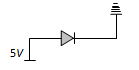
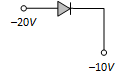
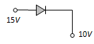
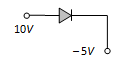
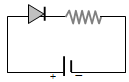
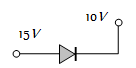
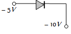
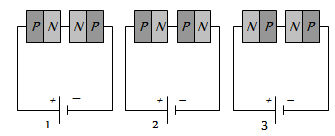
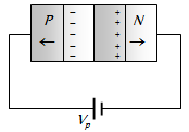
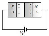
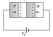
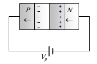
Two PN-junctions can be connected in series by three different methods as shown in the figure. If the potential difference in the junctions is the same, then the correct connections will be
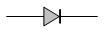
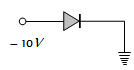
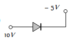
A semiconductor device is connected in a series circuit with a battery and a resistance. A current is found to pass through the circuit. If the polarity of the battery is reversed, the current drops almost to zero. The device may be
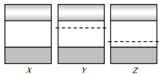
Carbon, silicon and Germanium atoms have four valence electrons each. Their valence and conduction band are separated by energy band gaps represented by $\left(E_g\right)_C \cdot\left(E_g\right)_{s i}$ and $\left(E_g\right)_{G e}$ respectively. Which one of the following relationship is true in their case
✓
$\left(E_g\right) C>\left(E_g\right) Si$
B
$\left(E_g\right) C=\left(E_g\right) Si$
C
$\left( E _{ g }\right) C <\left( E _{ g }\right) Ge$
D
$\left( E _{ g }\right) C <\left( E _{ g }\right) Si$
The electron mobility in $N-$type germanium is $3900 \mathrm{~cm}^2 / \mathrm{v}-s$ and its conductivity is $6.24 \ \mathrm{mho} / \mathrm{cm}$, then impurity concentration will be if the effect of cotters is negligible