Questions

Assertion (A) & Reason (B) MCQ

Take a timed test

15 questions · 1 auto-graded MCQ + 14 self-marked written.

Question 11 Mark
 
Two statements are given-one labelled Assertion (A) and the other labelled Reason (R). Select the correct answer to these questions from thecodes(a), (b), (c) and (d) as given below.
  1. Both A and R are true and R is the correct explanation of A.
  2. Both A and R are true but R is not the correct explanation of A.
  3. A is true but R is false.
  4. A is false and R is also false.
Assertion: V - I characteristic of p-n diode is same as that of any other conductor.
Reason: p-n diode behave as conductor at room temperature.
Answer
  1. A is false and R is also false.
Explanation:
The V - I characteristic of p-n di ode depends whether the junction is forward biased or reverse biased. This can be showed by graph between voltage and current.

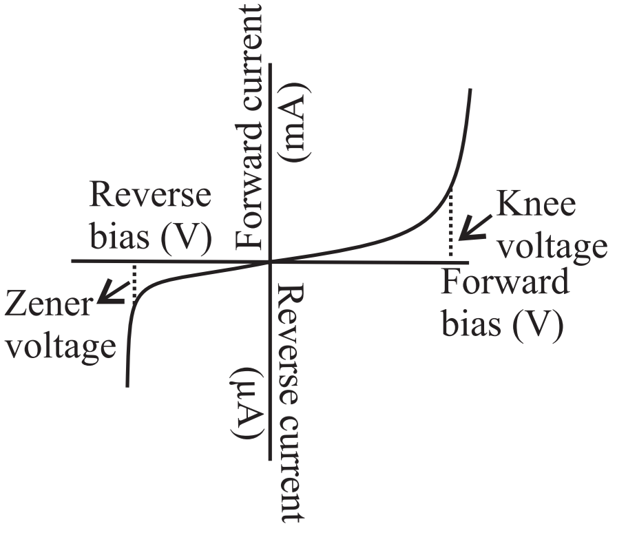
In the given graph knee voltage is a voltage at which forward bias becomes greater than the potential barrier, the forward current increases almost linearly, where as zener voltage is a voltage at which reverse current increases suddenly. From this graph we can verify that p-n diode characteristics are very different from that of conductor which obey's Ohm's law.
View full question & answer
Question 21 Mark
Two statements are given-one labelled Assertion (A) and the other labelled Reason (R). Select the correct answer to these questions from thecodes(a), (b), (c) and (d) as given below.
  1. Both A and R are true and R is the correct explanation of A.
  2. Both A and R are true but R is not the correct explanation of A.
  3. A is true but R is false.
  4. A is false and R is also false.
Assertion: Diode lasers are used as optical sources in optical communicatiod.
Reason: Diode lasers consume less energy.
Answer
  1. Both A and R are true and R is the correct explanation of A.
Explanation:
In optical communication, a semiconductor bases laser (diode laser) is used to generate analog signals or digital pulses for transmission through optical fibres. The advantages of diode lasers are their small size and low power input.
View full question & answer
Question 31 Mark
Two statements are given-one labelled Assertion (A) and the other labelled Reason (R). Select the correct answer to these questions from thecodes(a), (b), (c) and (d) as given below.
  1. Both A and R are true and R is the correct explanation of A.
  2. Both A and R are true but R is not the correct explanation of A.
  3. A is true but R is false.
  4. A is false and R is also false.
Assertion: Diamond behaves like an insulator.
Reason: There is a large energy gap between valence band and conduction band of diamond.
Answer
  1. Both A and R are true and R is the correct explanation of A.
Explanation:
In insulator, the forbidden energy gap is quite large. When electric field is applied to such a solid, the electron find it difficult to acquire such a large amount of energy. Thus no electron flow occurs.
View full question & answer
Question 41 Mark
Two statements are given-one labelled Assertion (A) and the other labelled Reason (R). Select the correct answer to these questions from thecodes(a), (b), (c) and (d) as given below.
  1. Both A and R are true and R is the correct explanation of A.
  2. Both A and R are true but R is not the correct explanation of A.
  3. A is true but R is false.
  4. A is false and R is also false.
Assertion: In a semiconductor diode, the reverse biased current is due to drift of free electrons and holes.
Reason: The drift of electrons and holes is due to thermal excitation.
Answer
  1. Both A and R are true but R is not the correct explanation of A.
Explanation:
A reverse bias on a p-n junction opposes the movement of the majority charge carriers thus stopping the diffusion current. It makes the free electrons and holes to drift cross the junction. Therefore a small current in $\mu\text{A}$ flows even when the p-n junction is reverse biased. The drift current is due to the thermal excitations of the electrons and holes.
View full question & answer
Question 51 Mark
Two statements are given-one labelled Assertion (A) and the other labelled Reason (R). Select the correct answer to these questions from thecodes(a), (b), (c) and (d) as given below.
  1. Both A and R are true and R is the correct explanation of A.
  2. Both A and R are true but R is not the correct explanation of A.
  3. A is true but R is false.
  4. A is false and R is also false.
Assertion: At absolute zero the conductivity of semiconductor is zero.
Reason: In a semiconductor there are no free electrons at any temperature.
Answer
  1. A is true but R is false.
Explanation:
In a semiconductor, there are no free electrons at 0K. The number of free electrons increases with increase in temperature because with increase in temperature the electron get sufficient energy to cross forbidden band and reach conduction band. But total number of free electrons in a semiconductor is less than that in a conductor.
View full question & answer
Question 61 Mark
Two statements are given-one labelled Assertion (A) and the other labelled Reason (R). Select the correct answer to these questions from thecodes(a), (b), (c) and (d) as given below.
  1. Both A and R are true and R is the correct explanation of A.
  2. Both A and R are true but R is not the correct explanation of A.
  3. A is true but R is false.
  4. A is false and R is also false.
Assertion: : The half-wave rectifier work only for positive half cycle of ac.
Reason: In half-wave rectifier only one diode is used.
Answer
  1. Both A and R are true and R is the correct explanation of A.
Explanation:
In half wave rectifier, the one diode is biased only when ac is in positive half of its cycle. For negative half of the ac cycle the diode is reversed biased and there is no output corresponding to that. Since for only one-half cycle we get a voltage output, because of which it is called half wave rectifier.
View full question & answer
Question 71 Mark
Two statements are given-one labelled Assertion (A) and the other labelled Reason (R). Select the correct answer to these questions from thecodes(a), (b), (c) and (d) as given below.
  1. Both A and R are true and R is the correct explanation of A.
  2. Both A and R are true but R is not the correct explanation of A.
  3. A is true but R is false.
  4. A is false and R is also false.
Assertion: The resistance of p-n junction is low when forward biased and is high when reverse biased.
Reason: In reversed biased, the depletion layer is reduced.
Answer
  1. A is true but R is false.
Explanation:
A small increase in forward voltage across p-n junction shows large increase in forward current. Hence the resistance $\Big(=\frac{\text{Voltege}}{\text{Current}}\Big)$ 0f p-n junction is low when forward biased. Also the width of depletion layer of p-n junction decreases in forward bias.
A large increase in reverse voltage across p-n shows small increase in reverse current. Hence the resistance of p-n junction is high when reverse biased. Also the width of the depletion layer of p-n junction increases in reverse biased.
View full question & answer
Question 81 Mark
Two statements are given-one labelled Assertion (A) and the other labelled Reason (R). Select the correct answer to these questions from thecodes(a), (b), (c) and (d) as given below.
  1. Both A and R are true and R is the correct explanation of A.
  2. Both A and R are true but R is not the correct explanation of A.
  3. A is true but R is false.
  4. A is false and R is also false.
Assertion: The depletion layer in the p-n junction is free from mobile charge carriers.
Reason: There is no electric field across the junction barrier.
Answer
  1. A is true but R is false.
Explanation:
Due to diffusion of holes from the p-region to the n-region and of electrons from the n-region to the p-region an electric field is set up across the junction barrier. Once the depletion layer is formed it is in equilibrium and becomes free of mobile charge carriers.
View full question & answer
MCQ 91 Mark
Two statements are given$-$one labelled Assertion $(A)$ and the other labelled Reason $(R).$ Select the correct answer to these questions from thecodes $(a), (b), (c)$ and $(d)$ as given below.
Assertion: Light Emitting Diode $\text{(LED)}$ emit spontaneous radiation.
Reason: $\text{LED}$ are forward-biased $p-n$ junction.
  • A
    Both $A$ and $R$ are true and $R$ is the correct explanation of $A.$
  • Both $A$ and $R$ are true but $R$ is not the correct explanation of $A.$
  • C
    $A$ is true but $R$ is false.
  • D
    $A$ is false and $R$ is also false.
Answer
Correct option: B.
Both $A$ and $R$ are true but $R$ is not the correct explanation of $A.$
In semiconductor there may be energy bands due to donor impurities $(E_D)$ near the conduction band or acceptor impurities $(E_A)$ near the valence band. When electron falls from higher to lower energy level containing holes, the energy is released in the form of radiation. The energy of radiation emitted by $\text{LED}$ is equal or less than the band gap of the semiconductor used. The radiation released lies in range of visible light whose colour depends on the semiconductor used.
View full question & answer
Question 101 Mark
Two statements are given-one labelled Assertion (A) and the other labelled Reason (R). Select the correct answer to these questions from thecodes(a), (b), (c) and (d) as given below.
  1. Both A and R are true and R is the correct explanation of A.
  2. Both A and R are true but R is not the correct explanation of A.
  3. A is true but R is false.
  4. A is false and R is also false.
Assertion: The probability of electrons to be found in the conduction band of an intrinsic semiconductor at a finite temperature decrease exponentially with increasing band gap.
Reason: It will be more difficult for the electron to cross over the large band gap while going from valence band to conduction band.
Answer
  1. Both A and R are true and R is the correct explanation of A.
Explanation:
For electron to jump from valence band to conduction band needs energy equal or more than the forbidden band between these two band. As the energy of band gap increases, it becomes difficult for electron to get that equivalent energy.
View full question & answer
Question 111 Mark
Two statements are given-one labelled Assertion (A) and the other labelled Reason (R). Select the correct answer to these questions from thecodes(a), (b), (c) and (d) as given below.
  1. Both A and R are true and R is the correct explanation of A.
  2. Both A and R are true but R is not the correct explanation of A.
  3. A is true but R is false.
  4. A is false and R is also false.
Assertion: At 0K, Germanium is a superconductor.
Reason: At 0K, Germanium offers zero resistance.
Answer
  1. A is false and R is also false.
Explanation:
At 0K, Germanium offers infinite resistance, and it behaves as an insulator.
View full question & answer
Question 121 Mark
Two statements are given-one labelled Assertion (A) and the other labelled Reason (R). Select the correct answer to these questions from thecodes(a), (b), (c) and (d) as given below.
  1. Both A and R are true and R is the correct explanation of A.
  2. Both A and R are true but R is not the correct explanation of A.
  3. A is true but R is false.
  4. A is false and R is also false.
Assertion: The dominant mechanism for motion of charge carriers in forward and reverse biase silicon p-n junction are drift in both forward and reverse bias.
Reason: In reverse biased, no current flow through the junction.
Answer
  1. A is false and R is also false.
Explanation:
In p-n junction, the diffusion of majority carriers takes place when junction is forward biased and drifting of minority carriers takes place across the junction, when reverse biased. The reverse bias opposes the majority carriers but makes the minority carriers to cross the p-n junction. Thus the small current in $\mu_\text{A}$ flows during reverse bias.
View full question & answer
Question 131 Mark
Two statements are given-one labelled Assertion (A) and the other labelled Reason (R). Select the correct answer to these questions from thecodes(a), (b), (c) and (d) as given below.
  1. Both A and R are true and R is the correct explanation of A.
  2. Both A and R are true but R is not the correct explanation of A.
  3. A is true but R is false.
  4. A is false and R is also false.
Assertion: Silicon is preferred over germanium for making semiconductor devices.
Reason: The energy band for germanium is more than the energy band of silicon.
Answer
  1. A is false and R is also false.
Explanation:
The energy gap for germanium is less (0.72eV) than the energy gap of silicon (I.IeV). Therefore, germanium is preferred over silicon for making semiconductor devices.
View full question & answer
Question 141 Mark
Two statements are given-one labelled Assertion (A) and the other labelled Reason (R). Select the correct answer to these questions from thecodes(a), (b), (c) and (d) as given below.
  1. Both A and R are true and R is the correct explanation of A.
  2. Both A and R are true but R is not the correct explanation of A.
  3. A is true but R is false.
  4. A is false and R is also false.
Assertion: The ratio of free electrons to holes in intrinsic semiconductor is greater than one.
Reason: The electrons are lighter particles and holes are heavy particles.
Answer
  1. Both A and R are true but R is not the correct explanation of A.
Explanation:
In intrinsic semiconductor $\frac{\text{n}_\text{e}}{\text{n}_\text{h}} = \text{I}$ and holes are not particles but vacancies created due to breakage of covalent bond.
View full question & answer
Question 151 Mark
Two statements are given-one labelled Assertion (A) and the other labelled Reason (R). Select the correct answer to these questions from thecodes(a), (b), (c) and (d) as given below.
  1. Both A and R are true and R is the correct explanation of A.
  2. Both A and R are true but R is not the correct explanation of A.
  3. A is true but R is false.
  4. A is false and R is also false.
Assertion: The resistivity of a semiconductor increases with temperature.
Reason: The atoms of a semiconductor vibrate with larger amplitude at higher temperatures thereby increasing its resistivity.
Answer
  1. A is false and R is also false.
Explanation:
With the increase of temperature, the average energy exchanged in a collision increases and so more valence electrons can cross the energy gap, thereby increasing the electron-hole pairs. As in a semiconductor, conduction occurs mainly through electron-hole pairs, so conductivity increases with increase of temperature. Which in turn implies that the resistivity of a semiconductor decreases with rise in temperature.
View full question & answer