Questions

2 Marks Questions

Take a timed test

51 questions · self-marked practice — reveal the answer and mark yourself.

Question 12 Marks
Two amplifiers are connected one after the other in series (cascaded). The first amplifier has a voltage gain of 10 and the second has a voltage gain of 20. If the input signal is 0.01 volt, calculate the output ac signal.
Answer
Voltage gain of the first amplifier, $\mathrm{V}_1=10$
Voltage gain of the second amplifier, $\mathrm{V}_2=20$
Input signal voltage, $\mathrm{V}_{\mathrm{i}}=0.01 \mathrm{~V}$
Output AC signal voltage $=\mathrm{V}_0$
The total voltage gain of a two-stage cascaded amplifier is given by the product of voltage gains of both the stages, i.e.,
$V=V_1 \times V_2 $
$ =10 \times 20=200$
We have the relation:
$\mathrm{V}=\frac{\mathrm{V}_0}{\mathrm{~V}_1} $
$ \mathrm{~V}_0=\mathrm{V} \times \mathrm{V}_{\mathrm{i}} $
$ =200 \times 0.01=2 \mathrm{~V}$
Therefore, the output AC signal of the given amplifier is 2 V .
View full question & answer
Question 22 Marks
In half-wave rectification, what is the output frequency if the input frequency is 50 Hz. What is the output frequency of a full-wave rectifier for the same input frequency.
Answer
Input frequency = 50 HzFor a half-wave rectifier, the output frequency is equal to the input frequency.
$\therefore$ Output frequency = 50 Hz
For a full-wave rectifier, the output frequency is twice the input frequency.
$\therefore$ Output frequency = 2 × 50 = 100 Hz
View full question & answer
Question 32 Marks
Explain, with the help of a circuit diagram, the working of a p-n junction diode as a half-wave rectifier.
Answer


Working:
During one half of the input AC, the diode is forward biased and a current flows through $R_L$.
During the other half of the input AC, the diode is reverse biased and no current flows through the load $R_L$.
Hence, the given AC input is rectified.
View full question & answer
Question 42 Marks
Draw a circuit diagram of n-p-n transistor amplifier in CE configuration. Under what condition does the transistor act as an amplifier?
Answer

Condition: The transistor must be operated close to the centre of its active region.
Alternate Answer
The base - Emitter junction of the transistor must be (suitably) forward biased and the collector – emitter junction must be (suitably) reverse biased.
View full question & answer
Question 52 Marks
Draw typical output characteristics of an n-p-n transistor in CE configuration. Show how these characteristics can be used to determine output resistance.
Answer
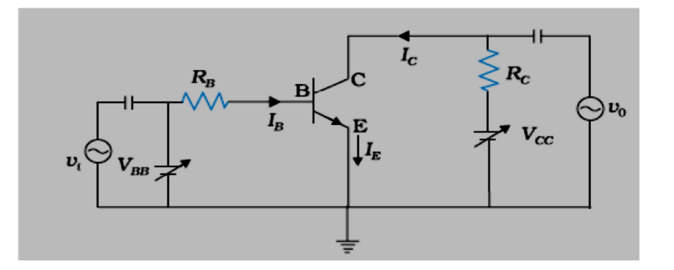
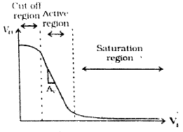
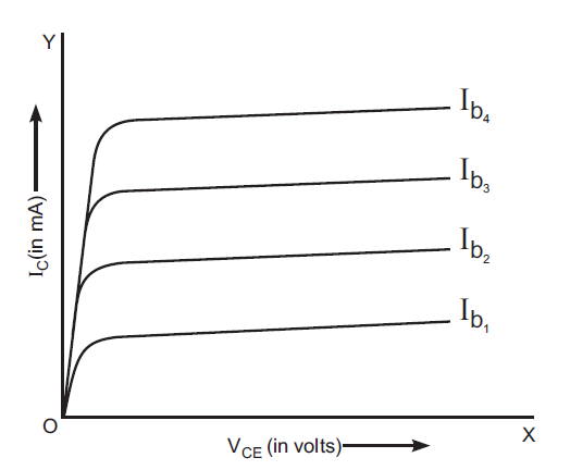
The reciprocal of the slope of the linear part of the output characteristics represents the output resistance.
$\text{r}_{0} = \bigg(\frac{\Delta\text{V}_{CE}}{\Delta\text{I}_{C}}\bigg)_{I_B4}$ (as shown in fig.).
View full question & answer
Question 62 Marks
  1. Identify the logic gates marked P and Q in the given logic circuit.
  1. Write down the output at X for the inputs A = 0, B = 0 and A = 1, B = 1.
Answer
  1. P: NAND gate.
Q: OR gate.
  1. Inputs A = 0 and B = 0 then output X=1
Inputs A = 1 and B = 1 then output X = 1.
View full question & answer
Question 72 Marks
Two semiconductor materials X and Y shown in the given figure, are made by doping germanium crystal with indum and arsenic respectively. The two are joined end to end and connected to a battery as shown.
  1. Will the junction be forward biased or reverse biased?
  2. Sketch a V-I graph for this arrangement.
Answer
(If X and Y are correctly identified but the identification of biasing is incorrect or not given at all, award.)
$(\text{X}\rightarrow\text{p} \text{Type})$
$(\text{Y}\rightarrow\text{n} \text{Type})$
  1. Reverse biased.
  2. Graph:
View full question & answer
Question 82 Marks
Describe, with the help of a circuit diagram, the working of a photodiode.
Answer

When photodiode is illuminated with light (photons), with energy $(hv > E_g)$ electron-hole pairs are generated near the depletion region of the diode. The direction of electric field is such that electrons reach n-side and holes reach p-side and give current(in reverse direction)
View full question & answer
Question 92 Marks
Write two points of difference between n-type and p-type semiconductors.
Answer
S.no n- type semiconductor p- type semiconductor
1 Pentavalent impurity is added. Trivalent impurity is added.
2 Electrons are the majority charge carrier/$(?_? >> ?_h)$ Holes are the majority charge carriers/$(?_h >> ?_?).$
3 New energy level formed near conduction band. New energy level formed near valence band.
View full question & answer
Question 102 Marks
Write two points of difference between intrinsic and extrinsic semiconductors.
Answer
Intrinsic Extrinsic
i. Pure semiconductor. i. Doped or impure.
ii. ?? = ?ℎ. ii. ?? ≠ ?ℎ.
iii. Low conductivity at room temperature. iii. Higher conductivity at room temperature.
iv. Conductivity depends on temperature. iv. Conductivity does not dependm significantly on temperature.
View full question & answer
Question 112 Marks
Distinguish between 'intrinsic' and 'extrinsic' semiconductors.
Answer
Intrinsic Semiconductor Extrinsic Semiconductor
(i) Without any impurity atoms. (i) Doped with trivalent/pentavalent impurity atoms.
(ii) $\text{n}_{e} =\text{n}_{h}$ (ii) $\text{n}_{e} \neq \text{n}_{h}$
View full question & answer
Question 122 Marks
Identify the logic gates marked 'P' and 'Q' in the given circuit. Write the truth table for the combination.
Answer
P: NAND Gate
Q: OR Gate
Truth Table
Input Output
A B X
0 0 1
1 0 1
0 1 1
1 1 1
View full question & answer
Question 132 Marks
Write the truth table for the combination of the gates shown. Name the gates used.
Answer
Input Output
A B Y' Y
0 0 0 0
0 1 1 0
1 0 1 1
1 1 1 1
Gate
R: OR Gate
S: AND Gate.
View full question & answer
Question 142 Marks

In the given circuit diagram, a voltmeter ‘V’ is connected aross a lamp ’L’. How would (i) the brightness of the lamp and (ii) voltmeter reading ‘V’ be affected, if the value of resistance ‘R’ is decreased? Justify your answer.
Answer
  1. Increases. As the value of the base current increases, the collect or current will increase proportionately.
  2. Increases. Due to increase in collect or current, voltage drop across lamp will increase.
View full question & answer
Question 152 Marks
The current in the forward bias is known to be more $(\sim\mu\text{A})$ than the current in the reverse bias $(\sim\mu\text{A})$.What is the reason, then, to operate the photodiode in reverse bias?
Answer
Even though the current in forward bias has a larger magnitude, the change, due to changes in light intensity, in the minority carrier dominated reverse bias current, is more and is, therefore, more easily detectable.
View full question & answer
Question 162 Marks
Draw the transfer characteristic curve of a base biased transistor in CE configuration. Explain clearly how the active region of the $\mathrm{V}_0$ versus $\mathrm{V}_{\mathrm{i}}$ curve in a transistor is used as an amplifier.
Answer


In the active region, a (small) increase of $V_i$ results in a (large, almost linear) increase in $I_c$, This results in an increase in the voltage drop, This results in an increase in the voltage drop cross $R_c$.
View full question & answer
Question 172 Marks
Name the semiconductor device that can be used to regulate an unregulated dc power supply. With the help of I-V characteristics of this device, explain its working principle.
Answer
Zener diode.Alternate Answer

I-V characteristic

insigniticant change in the (reverse) bias voltage across the Zener diode (and hence the load) even for large changes in current.
View full question & answer
Question 182 Marks
Draw the circuit diagram of an illuminated photodiode in reverse bias. How is photodiode used to measure light intensity?
Answer
Circuit diagram of an illuminated photodiode:
Explanation:
The magnitude of the photo current depends on the intensity of incident light (photo current is proportional to incident light intensity). Thus photo diode can be used to measure light intensity.
View full question & answer
Question 192 Marks
The following figure shows the input waveforms (A, ,B) and the output waveform (Y) of a gate. Identify the gate, write its truth table and draw its logic symbol.
Answer
NAND Gate
INPUT OUTPUT
A B Y
0 0 1
0 1 1
1 0 1
1 1 0
View full question & answer
Question 202 Marks
The given inputs A, B are fed to a 2-input NAND gate. Draw the output wave form of the gate.
Answer
Writing truth table.
A B Y
0 0 1
0 1 0
1 0 0
1 1 0
View full question & answer
Question 212 Marks
Distinguish between an intrinsic semiconductor and P-type semiconductor. Give reason, why, a P-type semiconductor crystal is electrically neutral, although$\text{n}_{h}>>\text{n}_{e}$.
Answer
  1. Intrinsic semiconductor does not contain any impurity while p-type semiconductor is doped with a trivalent impurity.
Alternate Answer

For an intrinsic semiconductor, $\text{n}_{e} = \text{n}_{h}$ while for a p-type semiconductor $\text{n}_{h}>>\text{n}_{e}$or any other difference.

Alternate Answer

Shows the distinction by band diagram.

(HOTS)
  1. p-type semiconductor is made by doping the neutral intrinsic semicondustor with trivalent impurity atoms.
View full question & answer
Question 222 Marks
The output of an OR gate is connected to both the inputs of a NAND gate. Draw the logic circuit of this combination of getes and write its truth table.
Answer

A B Y Y
0 0 0 1
0 1 1 0
1 0 1 0
1 1 1 0
View full question & answer
Question 232 Marks
Explain how the width of depletion layer in a p-n junction diode changes when the junction is (i) forward biased (ii) reverse biased.
Answer
  1. In forward biasing, the depletion layer decreases.
Reason: Majority charge carriers come closer to junction.
  1. In reverse biasing, the width of depletion layer increases.
Reason: The majority charge carries go farther away from the junction.
View full question & answer
Question 242 Marks
Draw and explain the output waveform across the load resistor R, if the input waveform is as shown in the given figure.
Answer
If the candidate considers it as a circuit containing diode.Wave form:

Explanation:
When the input voltage is +5v, the diode, being forward biased, conducts and output is obtained across R. When the input is –5v, the diode being reverse biased does not conduct and hence there is no output.
Alternate Answer
If the candidate considers it as a circuit with NOT gate.
Wave form:

Explanation:
When the input is zero, NOT gate conducts and output is obtained across R.
When the input is 5V there will be no output.
Alternate Answer
Output waveform:
View full question & answer
Question 252 Marks
Explain the terms ‘depletion layer’ and ‘potential barrier’ in a p-n junction diode. How are the (a) Width of depletion layer, and (b) Value of potential barrier affected when the p-n junction is forward biased?
Answer
Depletion layer: It is a layer of immobile ions formed near the p-n junction by diffusion of majority charge carriers and electron-hole recombination.
Potential barrier: It is the potential difference developed across the junction when diffusion current & drift current attains equilibrium across the junction.
  1. When forward biased, width of depletion layer decreases.
  2. And value of barrier potential also reduces as $v_0- v.$
View full question & answer
Question 262 Marks
A semiconductor has equal electron and hole concentration of $6 \times 10^8 / \mathrm{m}^3$. On doping with certain impurity, electron concentration increases to $9 \times 10^{12} / \mathrm{m}^3$.
  1. Identify the new semiconductor obtained after doping.
  2. Calculate the new hole concentration.
Answer
  1. The doped semiconductor is n-type.
  2. $\text{n}_\text{e}\text{n}_\text{h}=\text{n}^2_\text{i}$
$\Rightarrow\text{n}_\text{h}=\frac{\text{n}^2_\text{i}}{\text{n}_\text{e}}$
$=\frac{(6\times10^8)^2}{9\times10^{12}}=4\times10^4\text{per m}^3$
View full question & answer
Question 272 Marks
Why are elemental dopants for Silicon or Germanium usually chosen from group XIII or group XV?
Answer
The size of dopant atoms should be such as not to distort the pure semiconductor lattice structure and yet easily contribute a charge carrier on forming co-valent bonds with Si or Ge.
View full question & answer
Question 282 Marks
Germanium and silicon junction diodes are connected in parallel. A resistance R, a 12V battery, a milliammeter (mA) and key (K) are connected in series with them (figure). When key (K) is closed, a current begins to flow in the milliammeter. What will be the maximum reading of voltmeter connected across resistance R?
Answer
The potential barrier of germanium junction diode is 0.3V and of silicon is 0.7V. Both germanium and silicon are forward biased. Therefore, for conduction the minimum potential difference across junction diode is 0.3V.
Maximum reading of voltmeter connected across R = 12 - 0.3 = 11.7V.
View full question & answer
Question 292 Marks
The drift current in a p-n junction is $20.0\mu\text{A}.$ Estimate the number of electrons crossing a cross-section per second in the depletion region.
Answer
Drift current $=20\mu\text{A}=20\times10^{-6}\text{A}$
Both holes and electrons are moving
So, no.of electrons $=\frac{20\times10^{-6}}{2\times1.6\times10^{-19}}=6.25\times10^{13}.$
View full question & answer
Question 302 Marks
Calculate the current through the circuit and the potential difference across the diode shown in figure. The drift current for the diode is $20\mu\text{A}.$
Answer

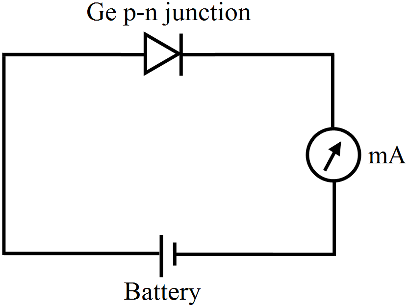
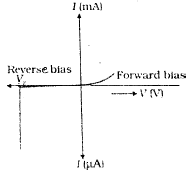
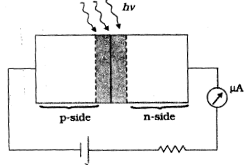
Current in the circuit = Drift current
(Since, the diode is reverse biased $=20\mu\text{A})$
Voltage across the diode $=5-\big(20\times20\times10^{-6}\big)$
$=5-\big(4\times10^{-4}\big)=5\text{V}.$
View full question & answer
Question 312 Marks
Draw a p-n junction which is reverse biased.
Answer
The p-n junction with reverse bias is shown in figure.
View full question & answer
Question 322 Marks
What are the readings of the ammeters $A_1$ and $A_2$ shown in figure. Neglect the resistance of the meters.
Answer
The diode is reverse biased. Hence the resistance is infinite. So, current through $A_1$ is zero.

For $A_2$, current $=\frac{2}{10}=0.2\text{Amp}.$
View full question & answer
Question 332 Marks
Find the maximum wavelength of electromagnetic radiation which can create a hole-electron pair in germanium. The band gap in germanium is 0.65eV.
Answer
Given,
Band gap of germanium, E = 0.65eV
Wavelength of the incident radiation, $\lambda=?$
For the electron‒hole pair creation, the energy of the incident radiation should be at least equal to the band gap of the material.
So,
$\text{E}=\frac{\text{hc}}{\lambda}$
$\Rightarrow\lambda=\frac{\text{hc}}{\text{E}}=\frac{1242\text{eV}-\text{nm}}{0.65\text{eV}}$
$\Rightarrow\lambda=1910.7\times10^{-9}\text{m}$
$\Rightarrow\lambda=1.9\times10^{-5}\text{m}$
View full question & answer
Question 342 Marks
Name the logic gate which can be realised by using a p-n junction diode in the given diagram. Give its logic symbol and write the truth table. Name the gate which will be obtained by combining with a NOT gate.
Answer
The logic gate shown in the circuit diagram is OR gate.

Symbol of OR gate:
Input
 
Output
A
B
Y
0
0
1
1
0
1
0
1
1
1
1
1
The gate obtained by combining OR gate with NOT gate will be NOR gate.
View full question & answer
Question 352 Marks
A germanium p-n junction is connected to a battery with milliammeter in series. What should be the minimum voltage of battery so that current may flow in the circuit?
Answer
The internal potential barrier of germanium is 0.3V, therefore to overcome this barrier the potential of battery should be equal to or more than 0.3V.Therefore, the minimum voltage of battery = 0.3V.
View full question & answer
Question 362 Marks
Suppose the energy liberated in the recombination of a hole-electron pair is converted into electromagnetic radiation. If the maximum wavelength emitted is 820nm, what is the band gap?
Answer
Given,
Wavelength, $\lambda = 820\text{nm}$
The minimum energy released in the recombination of a conduction band electron with a valence band hole is equal to the band gap of the material.
Band gap, $\text{E}=\frac{\text{hc}}{\lambda}$
$\Rightarrow\text{E}=\frac{1240}{820}\frac{\text{eV}-\text{nm}}{\text{nm}}$
$\Rightarrow\text{E}=1.5\text{eV}$
View full question & answer
Question 372 Marks
The given inputs A and B are fed to 2-inputs NAND gate. Draw the output waveform of the gate.
Answer
The output waveform is as shown:
View full question & answer
Question 382 Marks
State the factor, which controls (i) wavelength of light and (ii) intensity of light, emitted by a LED.
Answer
  1. Wavelength of light emitted depends on its band energy gap.
  2. Intensity of light emitted depends on the forward current conducted by the p–n junction.
View full question & answer
Question 392 Marks
State with reason why a photodiode is usually operated at a reverse bias.
Answer
The fractional change due to incident light on minority charge carriers in reverse bias is much more than that over the majority charge carriers in forward bias. This charge in reverse bias current is more easily measurable. So, photodiodes are used to measure the intensity in reverse bias condition.
View full question & answer
Question 402 Marks
Each of the resistances shown in figure. has a value of $20\Omega.$ Find the equivalent resistance between A and B. Does it depend on whether the point A or B is at higher potential?
Answer
From the figure.

According to wheat stone bridge principle, there is no current through the diode.
Hence net resistance of the circuit is $\frac{40}{2}=20\Omega.$
View full question & answer
Question 412 Marks
An ac input signal of frequency 60Hz is rectified by a (i) half wave (ii) full wave rectifier. Draw the output waveform and write the output frequency in each case.
View full question & answer
Question 422 Marks
Can the potential barrier across a p-n junction be measured by simply connecting a voltmeter across the junction?
Answer
No, because the voltmeter must have a resistance very high compared to the junction resistance, the latter being nearly infinite.
View full question & answer
Question 432 Marks
State the reason, why GaAs is most commonly used in making a solar cell.
Answer
For solar cell, incident photon energy must be greater than band gap energy, i.e, $(hv > Eg) For GaAs, Eg = 1.43eV = 1.43eV$ and high optical absorption $\approx 104 cm^{-1}$, which are main criteria for fabrication of solar cells.
View full question & answer
Question 442 Marks
A modulating signal is a square wave, as shown in Fig.

The carrier wave is given by c(t) = 2sin (8$\pi$t) volts.
  1. Sketch the amplitude modulated waveform,
  2. What is the modulation index?
Answer
  1. The amplitude modulated waveform is given by superimposition of modulating signal on carrier wave and is shown below:
  1. We have,
$A_m=1 \mathrm{~V}, A_c=2 \mathrm{~V}$
Therefore, modulation index is given by,
$\mu=\frac{\text{A}_{\text{m}}}{\text{V}_\text{C}}=\frac{1}{2}=0.5$
View full question & answer
Question 452 Marks
The energy gaps in the energy band diagrams of a conductor, semiconductor and insulator are $\mathrm{E}_1, \mathrm{E}_2$ and $\mathrm{E}_3$. Arrange them in increasing order.
Answer
The energy gap in a conductor is zero, in a semiconductor is $\approx 1 \mathrm{eV}$ and in an insulator is $\geq 3 \mathrm{eV}$.
$ \therefore \mathrm{E}_1=0, \mathrm{E}_2 $
$ =1 \mathrm{eV}, \mathrm{E}_3 \geq 3 \mathrm{eV}$
$ \therefore \mathrm{E}_1 < \mathrm{E}_2 < \mathrm{E}_3$
View full question & answer
Question 462 Marks
Draw the output waveform across the resistor (Fig).
Answer
The diode act as a half wave rectifier, it offers low resistance when forward biased and high resistance when reverse biased. So the output is obtained only when positive input is given,so the output waveform is,
View full question & answer
Question 472 Marks
What is the resistance of an intrinsic semiconductor at 0K?
Answer
At 0K, the valence band is full and the conduction band is empty. As no electron is available for conduction in an intrinsic semiconductor, the intrinsic semiconductor at 0K acts as an insulator and hence offers infinite resistance.
View full question & answer
Question 482 Marks
Define trans conductance of a transistor.
Answer
The trans conductance of a transistor is defined as the ratio of the change in collector current to the change in base voltage at constant collector voltage.
$\text{gm}=\Big(\frac{\Delta\text{I}_\text{C}}{\Delta\text{V}_\text{b}}\Big)_{\text{V}_\text{C}=\text{Cons}\tan\text{t}}$
View full question & answer
Question 492 Marks
What type of extrinsic semiconductor is formed when:
  1. Germanium is doped with indium?
  2. Silicon is doped with bismuth?
Answer
  1. Indium is trivalent, so germanium doped with indium is an p-type semiconductor.
  2. Bismuth is pentavalent, so silicon doped with bismuth is a n-type semiconductor.
View full question & answer
Question 502 Marks
Can we measure the potential difference across an unbiased p–n junction by connecting a sensitive voltmeter across it?
Answer
No, the reason is there are no free charge carriers in the depletion region. Hence, in the absence of any external battery, there is no current flowing through the junction.
View full question & answer
Question 512 Marks
The $V-I$ characteristic of a silicon diode is shown in the Fig. 14.17. Calculate the resistance of the diode at (a) $I_D=15 mA$ and (b) $V_D=-10 V$.
Image
Answer
Considering the diode characteristics as a straight line between $I=10 mA$ to $I=20 mA$ passing through the origin, we can calculate the resistance using Ohm's law.
(a) From the curve, at $I=20 mA , V=0.8 V ; I=10 mA , V=0.7 V$ $r_{f b}=\Delta V / \Delta I=0.1 V / 10 mA =10 \Omega$
(b) From the curve at $V =-10 V , I=-1 \mu A$, Therefore,
$
r_{r b}=10 V / 1 \mu A =1.0 \times 10^7 \Omega
$
View full question & answer