In a good conductor the energy gap between the conduction band and the valence band is
[KCET 1993; EMCET (Med.) 1994]


Download our appand get started for free
Experience the future of education. Simply download our apps or reach out to us for more information. Let's shape the future of learning together!No signup needed.*
Similar Questions
- 1Plate resistance of two triode valves is $2 k \Omega$ and $4 k \Omega$, amplification factor of each of the valves is $40.$ The ratio of voltage amplification, when used with $4 k \Omega$ load resistance, will beView Solution
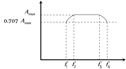
- 2The frequency response curve of $R C$ coupled amplifier is shown in figure. The band width of the amplifier will beView Solution
- 3View SolutionIn a junction diode, the holes are due to
- 4When $G e$ crystals are doped with phosphorus atom, then it becomesView Solution
- 5No bias is applied to a $P-N$ junction, then the currentView Solution
- 6On adjusting the $P-N$ junction diode in forward biasedView Solution
- 7View SolutionThe maximum efficiency of full wave rectifier is
- 8In the forward bias arrangement of a $P N$-junction diodeView Solution
- 9The curve between the work function of a metal $\left(\phi_o\right)$ and its temperature $(T)$ will beView Solution
- 10Barrier potential of a $P-N$ junction diode does not depend onView Solution