In the forward bias arrangement of a $P N$-junction diode
[MP PMT 1994, 96, 99]


Download our appand get started for free
Experience the future of education. Simply download our apps or reach out to us for more information. Let's shape the future of learning together!No signup needed.*
Similar Questions
- 1View SolutionThe state of the energy gained by valance electrons when the temperature is raised or when electric field is applied is called as
- 2In a $P N P$ transistor working as a common-base amplifier, current gain is $0.96$ and emitter current is $7.2\ mA$. The base current isView Solution
- 3View SolutionFor non-conductors, the energy gap is
- 4The impurity atoms which are mixed with pure silicon to make a $P$ type semiconductor are those ofView Solution
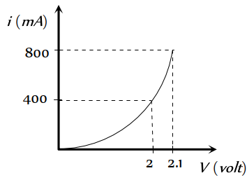
- 5The $i-V$ characteristic of a $P-N$ junction diode is shown below. The approximate dynamic resistance of the $P-N$ junction when a forward bias of $2$ volt is appliedView Solution
- 6The electrical circuit used to get smooth $d c$ output from a rectifier circuit is calledView Solution
- 7The cause of the potential barrier in a $P-N$ diode isView Solution
- 8View SolutionIn a junction diode, the holes are due to
- 9View SolutionThe electrical resistance of depletion layer is large because
- 10A semiconductor $X$ is made by doping a germanium crystal with arsenic $(Z=33)$. A second semiconductor $Y$ is made by doping germanium with indium $(Z=49)$. The two are joined end to end and connected to a battery as shown. Which of the following statements is correctView Solution