The reason of current flow in $P-N$ junction in forward bias is
[RPMT 2000]


Download our appand get started for free
Experience the future of education. Simply download our apps or reach out to us for more information. Let's shape the future of learning together!No signup needed.*
Similar Questions
- 1View SolutionThe introduction of a grid in a triode valve affects plate current by [CPMT 1975, 90]
- 2When plate voltage in diode valve is increased from $100$ volt to $150$ volt then plate current increases from $7.5\ mA$ to $12\ mA$. The dynamic plastic resistance will beView Solution
- 3View SolutionFor germanium crystal, the forbidden energy gap in joules is
- 4To make a $\text{PN}$ junction conductingView Solution
- 5Carbon, silicon and Germanium atoms have four valence electrons each. Their valence and conduction band are separated by energy band gaps represented by $(E) .(E)$ and $(E)$ respectively. Which one of the following relationship is true in their caseView Solution
- 6The curve between the work function of a metal $\left(\phi_o\right)$ and its temperature $(T)$ will beView Solution
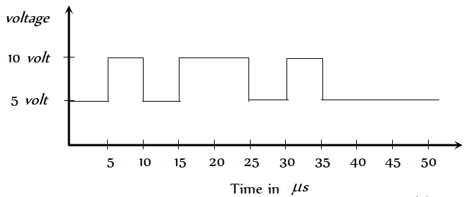
- 7View SolutionIn a negative logic the following wave form corresponds to the
- 8View SolutionIn extrinsic semiconductors
- 9View SolutionZener diode is used as
- 10In a $P-N$ junction diode if $P$ region is heavily doped than $n$ region then the depletion layer isView Solution