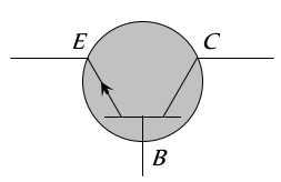
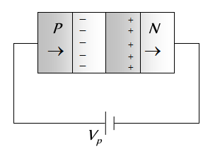
In a $P N$-junction
[CBSE PMT 2002


Download our appand get started for free
Experience the future of education. Simply download our apps or reach out to us for more information. Let's shape the future of learning together!No signup needed.*
Similar Questions
- 1View SolutionElectric current is due to drift of electrons in
- 2View SolutionSelect the correct statement
- 3View SolutionIn a semiconductor the separation between conduction band and valence band is of the order of
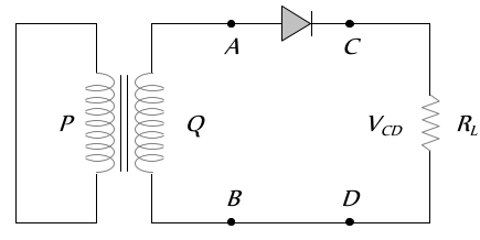
- 4In the half-wave rectifier circuit shown. Which one of the following wave forms is true for $V_{C D}$, the output across $C$ and $D$ ?View Solution
- 5The approximate ratio of resistances in the forward and reverse bias of the $P N$-junction diode isView Solution
- 6The depletion layer in silicon diode is $1 \mu m$ wide and the knee potential is $0.6 V$, then the electric field in the depletion layer will beView Solution
- 7View SolutionSymbolic representation of photodiode is
- 8View SolutionA full wave rectifier circuit along with the input and output voltages is shown in the figure Output voltage
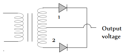
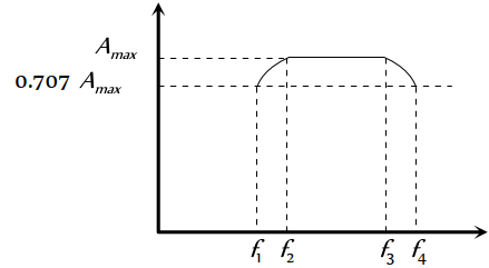
The contribution to output voltage from diode -2 is - 9The frequency response curve of $R C$ coupled amplifier is shown in figure. The band width of the amplifier will beView Solution
- 10View SolutionThe symbol given in figure represents