The symbol given in figure represents
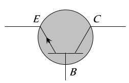
[AMU 1995, 96]


Download our appand get started for free
Experience the future of education. Simply download our apps or reach out to us for more information. Let's shape the future of learning together!No signup needed.*
Similar Questions
- 1$N$-type semiconductors will be obtained, when germanium is doped withView Solution
- 2View SolutionWhich one is in forward bias
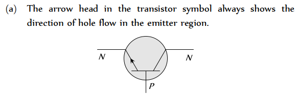
- 3In the study of transistor as an amplifier, if $\alpha=I_c / I_e$ and $\beta=I_c / I_b$, where $I_c, I_b$ and $l$ are the collector, base and emitter currents, thenView Solution
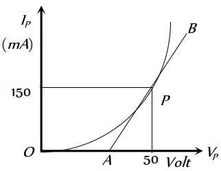
- 4The plate characteristic curve of a diode in space charge limited region is as shown in the figure. The slope of curve at point $P$ is $5.0 m A / V$. The static plate resistance of diode will beView Solution
- 5In a $P N P$ transistor working as a common-base amplifier, current gain is $0.96$ and emitter current is $7.2\ mA$. The base current isView Solution
- 6In a $P$-type semiconductor, germanium is doped withView Solution
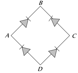
- 7In the diagram, the input is across the terminals $A$ and $C$ and the output is across the terminals $B$ and $D$, then the output isView Solution
- 8The dominant mechanisms for motion of charge carriers in forward and reverse biased silicon $P-N$ junctions areView Solution
- 9The energy gap of silicon is $1.14\ eV$. The maximum wavelength at which silicon will begin absorbing energy isView Solution
- 10View SolutionThe most commonly used material for making transistor is