A full wave rectifier circuit along with the input and output voltages is shown in the figure Output voltage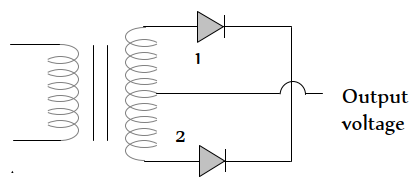
The contribution to output voltage from diode -2 is
The contribution to output voltage from diode -2 is
[MP PMT 2001]


Download our appand get started for free
Experience the future of education. Simply download our apps or reach out to us for more information. Let's shape the future of learning together!No signup needed.*
Similar Questions
- 1The energy gap of silicon is $1.14\ eV$. The maximum wavelength at which silicon will begin absorbing energy isView Solution
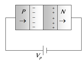
- 2Consider the following statements $A$ and $B$ and identify the correct choice of the given answers$A$ : The width of the depletion layer in a $P-N$ junction diode increases in forwards bias$B$ : In an intrinsic semiconductor the fermi energy level is exactly in the middle of the forbidden gapView Solution
- 3Which is the wrong statement in following sentences? A device in which $P$ and $N$-type semiconductors are used is more useful then a vacuum type becauseView Solution
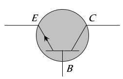
- 4View SolutionThe symbol given in figure represents
- 5The amplification factor of a triode is $18$ and its plate resistance is $8 \times 10 \Omega$. A load resistance of $10 \Omega$ is connected in the plate circuit. The voltage gain will beView Solution
- 6A piece of copper and the other of germanium are cooled from the room temperature to $80 K$, then which of the following would be a correct statementView Solution
- 7View SolutionSerious draw back of the semiconductor device is
- 8Two $P N$-junctions can be connected in series by three different methods as shown in the figure. If the potential difference in the junctions is the same, then the correct connections will beView Solution
- 9View SolutionA crystal diode is a
- 10View SolutionOf the diodes shown in the following diagrams, which one is reverse biased