Rajasthan BoardEnglish MediumSTD 12 SciencePhysicsSemiconductor Electronic: Material, Devices And Simple Circuits1 Mark
Question
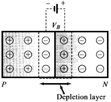
In the depletion region of a diode:
✓
Answer
On account of difference in concentration of charge carrier in the two sections of $P-N$ junction, the electrons from $N-$rcgion diffuse through the junction into $P-$region and the hole from $P-$region diffuse into $N-$region.
Due to diffusion, neutrality of both $N-$and $P-$type semiconductor is disturbed, a layer of negative charged ions appear near the junction in the $P-$crystal and a layer of positive ions appears near the junction in $N-$crystal.
This layer is called depletion layer.
The thickness of depletion layer is $1$ micron $= 10^{-6}m.$
Width of depletion layer $\infty 1/$Dopping
Depletion is directly proportional to temperature. Important point: The $P-N$ junction diode is equivalent to capacitor in which the depletion layer acts as a dielectric.
Need a full question paper?
Generate a complete, print-ready paper with questions like this in minutes — across 16+ boards, with answer keys.