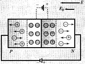
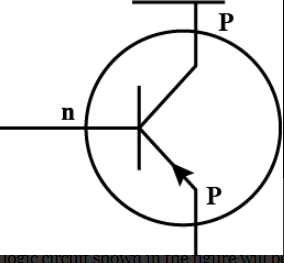
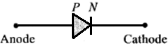
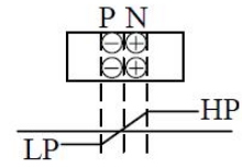
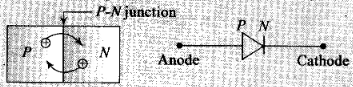
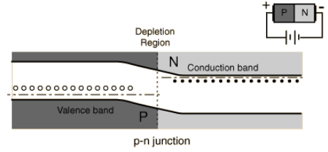
- From the p-side to the n-side.
Explanation:
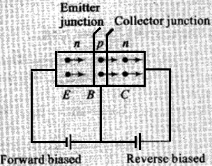
When a p‒n junction is formed then because of the difference in the concentration of charge carriers in the two regions, electrons from the n region move to the p region and holes from the p region move to the n region. Since the direction of the current is always opposite to the motion of electron, the direction of the current is from the p side to the n side.
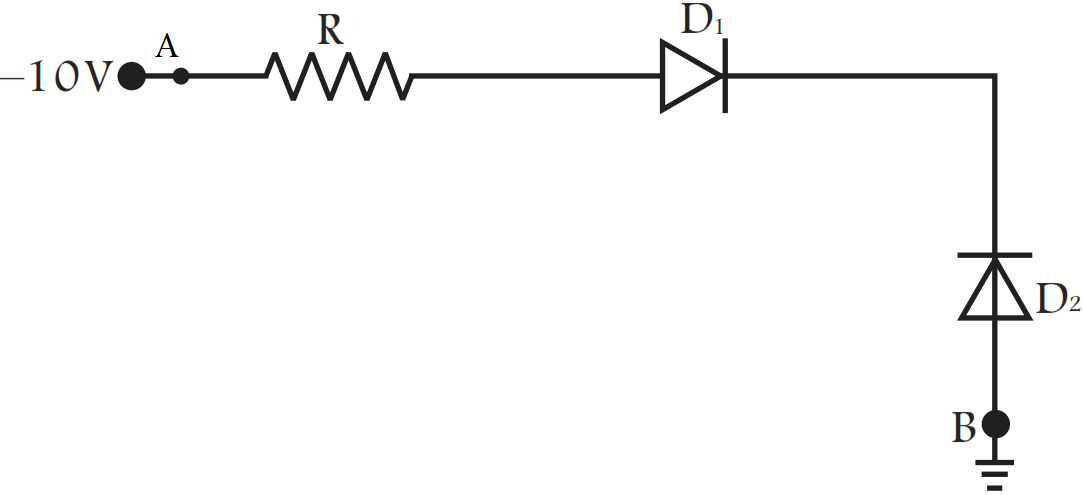
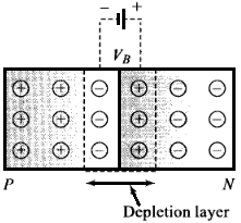
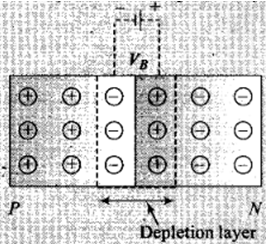
Similarly, when the junction is forward biassed, the positive terminal of the battery is connected to the pside of the p‒n junction and the negative terminal of the battery is connected to the n side of the p‒njunction. As a result, electrons in the n side of the p‒n junction are repelled by the negative terminal of the battery and they move to the p side, where the positive terminal of the battery attracts them. Similarly, holes from the p side of the p‒n junction are repelled by the positive terminal of the battery and they move to the n side, where the negative terminal of the battery attracts them. Thus, they give diffusion current from the p side to the n side across the p‒n junction.
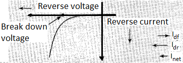
In reverse biassing, there is no flow of majority carriers across the junction; hence, there is not diffusion current. Here, the flow of majority carriers is opposed by the applied voltage.
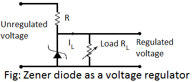
 Solution:
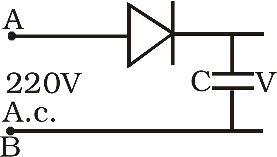