The cause of the potential barrier in a $P-N$ diode is
[CBSE PMT 1998; RPMT 2001]


Download our appand get started for free
Experience the future of education. Simply download our apps or reach out to us for more information. Let's shape the future of learning together!No signup needed.*
Similar Questions
- 1View SolutionNumber of secondary electrons emitted per number of primary electrons depends on
- 2View SolutionFor non-conductors, the energy gap is
- 3View SolutionFor germanium crystal, the forbidden energy gap in joules is
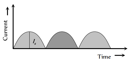
- 4View SolutionThe output current versus time curve of a rectifier is shown in the figure. The average value of the output current in this case is
- 5For a transistor, the current amplification factor is $0.8.$ The transistor is connected in common emitter configuration. The change in the collector current when the base current changes by 6 $m A$ isView Solution
- 6View SolutionWhich of the following semi-conductor diodes is reverse biased
- 7View SolutionWhich of the energy band diagrams shown in the figure corresponds to that of a semiconductor
- 8The amplification factor of a triode is $20.$ If the grid potential is reduced by $0.2$ volt then to keep the plate current constant its plate voltage is to be increased byView Solution
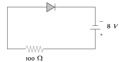
- 9A source voltage of $8 V$ drives the diode in fig. through a currentlimiting resistor of $100 ohm$. Then the magnitude of the slope load line on the $V-I$ characteristics of the diode isView Solution
- 10View SolutionCoating of strontium oxide on Tungsten cathode in a valve is good for thermionic emission because