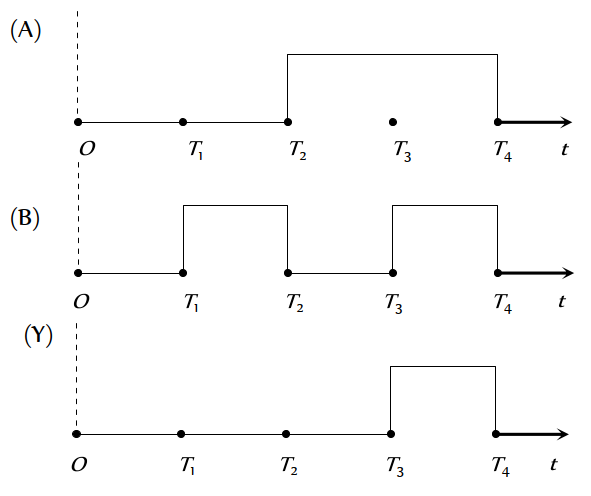
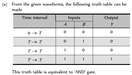
The given figure shows the wave forms for two inputs $A$ and $B$ and that for the output $Y$ of a logic circuit. The logic circuit is


Download our appand get started for free
Experience the future of education. Simply download our apps or reach out to us for more information. Let's shape the future of learning together!No signup needed.*
Similar Questions
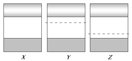
- 1View SolutionThe energy band diagrams for three semiconductor samples of silicon are as shown. We can then assert that
- 2The amplification factor of a triode is $18$ and its plate resistance is $8 \times 10 \Omega$. A load resistance of $10 \Omega$ is connected in the plate circuit. The voltage gain will beView Solution
- 3View SolutionEnergy bands in solids are a consequence of
- 4In $P$-N junction, the barrier potential offers resistance toView Solution
- 5View SolutionA semiconductor device is connected in a series circuit with a battery and a resistance. A current is found to pass through the circuit. If the polarity of the battery is reversed, the current drops almost to zero. The device may be
- 6Two $P N$-junctions can be connected in series by three different methods as shown in the figure. If the potential difference in the junctions is the same, then the correct connections will beView Solution
- 7When $N P N$ transistor is used as an amplifierView Solution
- 8View SolutionWhen phosphorus and antimony are mixed in zermaniun, then
- 9View SolutionSelect the correct statement
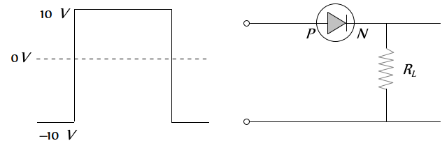
- 10If the following input signal is sent through a $P N$-junction diode, then the output signal across $R$ will beView Solution