The correct symbol for zener diode is
- A
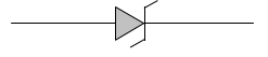
- B
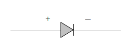
- C
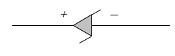
- D
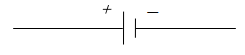
[RPMT 2000]


Download our appand get started for free
Experience the future of education. Simply download our apps or reach out to us for more information. Let's shape the future of learning together!No signup needed.*
Similar Questions
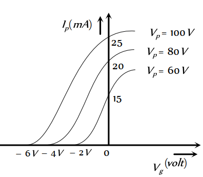
- 1View SolutionThe variation of anode current in a triode corresponding to a change in grid potential at three different values of the plate potential is shown in the diagram. The mutual conductance of the triode is
- 2In a triode amplifier, $\mu=25, r_p=40$ kilo ohm and load resistance $R_L=10$ kilo ohm. If the input signal voltage is $0.5$ volt, then output signal voltage will beView Solution
- 3In forward bias, the width of potential barrier in a $P-N$ junction diodeView Solution
- 4A $G e$ specimen is doped with $A l$. The concentration of acceptor atoms is $\sim 10^{-}$atoms $/ m$. Given that the intrinsic concentration of electron hole pairs is $\sim 10^{19} / m ^3$, the concentration of electrons in the specimen isView Solution
- 5View SolutionFor germanium crystal, the forbidden energy gap in joules is
- 6The valence of the impurity atom that is to be added to germanium crystal so as to make it a $N$-type semiconductor, isView Solution
- 7View SolutionSemiconductor is damaged by the strong current due to
- 8In a $P-N$ junction diode if $P$ region is heavily doped than $n$ region then the depletion layer isView Solution
- 9The width of forbidden gap in silicon crystal is $1.1\ eV$. When the crystal is converted in to a $N$-type semiconductor the distance of Fermi level from conduction band isView Solution
- 10The relation between $\alpha$ and $\beta$ parameters of current gains for a transistors is given byView Solution