The width of forbidden gap in silicon crystal is $1.1\ eV$. When the crystal is converted in to a $N$-type semiconductor the distance of Fermi level from conduction band is
[EAMCET (Med.) 1999]


Download our appand get started for free
Experience the future of education. Simply download our apps or reach out to us for more information. Let's shape the future of learning together!No signup needed.*
Similar Questions
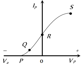
- 1View SolutionThe point representing the cut off grid voltage on the mutual characteristic of triode is
- 2When $G e$ crystals are doped with phosphorus atom, then it becomesView Solution
- 3View SolutionSerious draw back of the semiconductor device is
- 4View SolutionA crystal diode is a
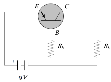
- 5In a transistor circuit shown here the base current is $35 \mu A$. The value of the resistor $R$ isView Solution
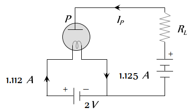
- 6View SolutionThe value of plate current in the given circuit diagram will be
- 7View SolutionIn a semiconductor the separation between conduction band and valence band is of the order of
- 8Thermionic emission from a heated filament varies with its temperature $T$ asView Solution
- 9The amplification factor of a triode is $20.$ If the grid potential is reduced by $0.2$ volt then to keep the plate current constant its plate voltage is to be increased byView Solution
- 10Different voltages are applied across a $P-N$ junction and the currents are measured for each value. Which of the following graphs is obtained between voltage and currentView Solution