The depletion layer in the $P-N$ junction region is caused by
[CBSE PMT 1994]


Download our appand get started for free
Experience the future of education. Simply download our apps or reach out to us for more information. Let's shape the future of learning together!No signup needed.*
Similar Questions
- 1View SolutionThe potential barrier, in the depletion layer, is due to
- 2Let $n_P$ and $n_e$ be the number of holes and conduction electrons respectively in a semiconductor. ThenView Solution
- 3View SolutionThe thermionic emission of electron is due to
- 4View SolutionThe introduction of a grid in a triode valve affects plate current by [CPMT 1975, 90]
- 5View SolutionThe triode constant is out of the following
- 6View SolutionThe electrical circuits used to get smooth d.c. output from a rectifier circuit is called
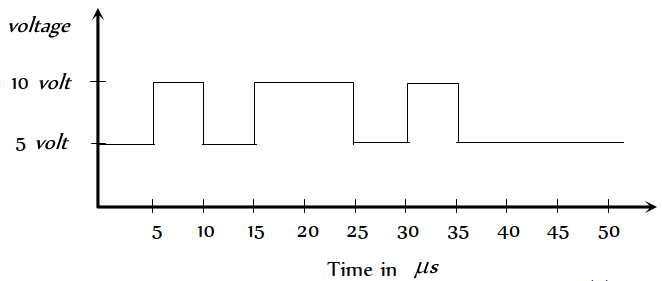
- 7View SolutionIn a negative logic the following wave form corresponds to the
- 8When $N$-type of semiconductor is heatedView Solution
- 9Wires $P$ and $Q$ have the same resistance at ordinary (room) temperature. When heated, resistance of $P$ increases and that of $Q$ decreases. We conclude thatView Solution
- 10The electrical circuit used to get smooth $d c$ output from a rectifier circuit is calledView Solution