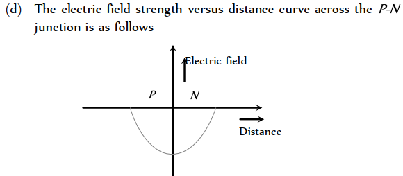
In the middle of the depletion layer of a reverse-biased $P N$ junction, the
[AIEEE 2003]


Download our appand get started for free
Experience the future of education. Simply download our apps or reach out to us for more information. Let's shape the future of learning together!No signup needed.*
Similar Questions
- 1In an $N P N$ transistor the collector current is $24 mA$. If $80 \%$ of electrons reach collector its base current in $m A$ isView Solution
- 2View SolutionThe mobility of free electron is greater than that of free holes because
- 3$N P N$ transistor are preferred to $P N P$ transistor because they haveView Solution
- 4Thermionic emission from a heated filament varies with its temperature $T$ asView Solution
- 5View SolutionTo a germanium sample, traces of gallium are added as an impurity. The resultant sample would behave like
- 6Plate voltage of a triode is increased from $200 V$ to $225 V$. To maintain the plate current, change in grid voltage from $5 V$ to $5.75 V$ is needed. The amplification factor isView Solution
- 7Carbon, silicon and Germanium atoms have four valence electrons each. Their valence and conduction band are separated by energy band gaps represented by $(E) .(E)$ and $(E)$ respectively. Which one of the following relationship is true in their caseView Solution
- 8View SolutionAt zero Kelvin a piece of germanium
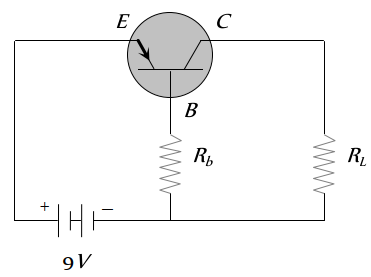
- 9In a transistor circuit shown here the base current is $35 \mu A$. The value of the resistor $R$ isView Solution
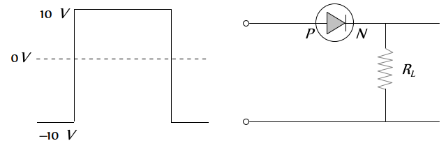
- 10If the following input signal is sent through a $P N$-junction diode, then the output signal across $R$ will beView Solution