The energy gap of silicon is $1.14\ eV$. The maximum wavelength at which silicon will begin absorbing energy is
[MP PMT 1993]


Download our appand get started for free
Experience the future of education. Simply download our apps or reach out to us for more information. Let's shape the future of learning together!No signup needed.*
Similar Questions
- 1$14 \times 10^{15}$ electrons reach the anode per second. If the power consumed is 448 milliwatts, then the plate (anode) voltage isView Solution
- 2The depletion layer in the $P-N$ junction region is caused byView Solution
- 3When $N P N$ transistor is used as an amplifierView Solution
- 4View Solution(USS 133) Indium impurity in germanium makes
- 5View SolutionIn a triode valve
- 6A $G e$ specimen is doped with $A l$. The concentration of acceptor atoms is $\sim 10^{-}$atoms $/ m$. Given that the intrinsic concentration of electron hole pairs is $\sim 10^{19} / m ^3$, the concentration of electrons in the specimen isView Solution
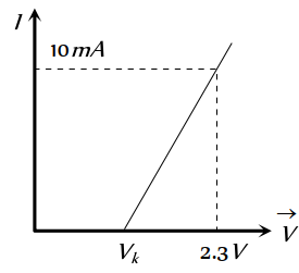
- 7The resistance of a germanium junction diode whose $V-I$ is shown in figure is $\left(V_k=0.3 V \right)$View Solution
- 8View Solutiondepending on the nature of impurity In intrinsic semiconductor at room temperature, number of electrons and holes are
- 9The dominant mechanisms for motion of charge carriers in forward and reverse biased silicon $P-N$ junctions areView Solution
- 10The reason of current flow in $P-N$ junction in forward bias isView Solution