The intrinsic semiconductor becomes an insulator at
[EAMCET (Med.) 1995; KCET (Engg./Med.) 1999;MP PET 2000; CBSE PMT 2001]


Download our appand get started for free
Experience the future of education. Simply download our apps or reach out to us for more information. Let's shape the future of learning together!No signup needed.*
Similar Questions
- 1View SolutionZener breakdown in a semi-conductor diode occurs when
- 2View SolutionWhich one of the following statements is not correct
- 3To obtain a $P$-type germanium semiconductor, it must be doped withView Solution
- 4View SolutionWhich of the following semi-conductor diodes is reverse biased
- 5View SolutionThe electrical resistance of depletion layer is large because
- 6The reverse biasing in a $P N$ junction diodeView Solution
- 7The correct curve between voltage gain $\left(A_v\right)$ and load resistance $\left(R_L\right)$ isView Solution
- 8Which is the wrong statement in following sentences? A device in which $P$ and $N$-type semiconductors are used is more useful then a vacuum type becauseView Solution
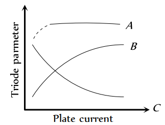
- 9The figure represents variation of triode parameter ( $\mu$ or $r$ or $g$ ) with the plate current. The correct variation of $\mu$ and $r$ are given, respectively by the curvesView Solution
- 10View SolutionSerious draw back of the semiconductor device is