Serious draw back of the semiconductor device is
[Pb. PMT 2004]


Download our appand get started for free
Experience the future of education. Simply download our apps or reach out to us for more information. Let's shape the future of learning together!No signup needed.*
Similar Questions
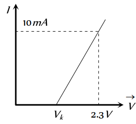
- 1The resistance of a germanium junction diode whose $V-I$ is shown in figure is $\left(V_k=0.3 V \right)$View Solution
- 2In an amplifier the load resistance $R_L$ is equal to the plate resistance $\left(r_p\right)$. The voltage amplification is equal toView Solution
- 3View SolutionThe band gap in Germanium and silicon in eV respectively is
- 4View SolutionWhich is the correct diagram of a half-wave rectifier
- 5View SolutionIn case of a semiconductor, which of the following statement is wrong
- 6In an experiment, the saturation in the plate current in a diode is observed at $240 V$. But a student still wants to increase the plate current. It can be done, ifView Solution
- 7$N P N$ transistor are preferred to $P N P$ transistor because they haveView Solution
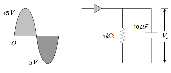
- 8View SolutionThe output in the circuit of figure is taken across a capacitor. It is as shown in figure
- 9View SolutionThe correct symbol for zener diode is
- 10View SolutionDiode is used as a/an