Which is the correct relation for forbidden energy gap in conductor, semi conductor and insulator
[RPMT 2001; AIEEE 2002]


Download our appand get started for free
Experience the future of education. Simply download our apps or reach out to us for more information. Let's shape the future of learning together!No signup needed.*
Similar Questions
- 1The relation between $\alpha$ and $\beta$ parameters of current gains for a transistors is given byView Solution
- 2View SolutionRegarding a semiconductor which one of the following is wrong
- 3The width of forbidden gap in silicon crystal is $1.1\ eV$. When the crystal is converted in to a $N$-type semiconductor the distance of Fermi level from conduction band isView Solution
- 4View SolutionWhich of the following statements is not true
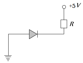
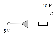
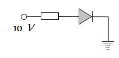
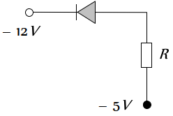
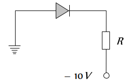
- 5View SolutionIn the given figure, which of the diodes are forward biased ?
- 6For a given triode $\mu=20$. The load resistance is $1.5$ times the anode resistance. The maximum gain will beView Solution
- 7The majority charge carriers in $P$-type semiconductor areView Solution
- 8View SolutionThe maximum efficiency of full wave rectifier is
- 9View SolutionSemiconductor is damaged by the strong current due to
- 10View SolutionZener breakdown takes place if