Questions · Page 2 of 9

M.C.Q (1 Marks)

Question 511 Mark

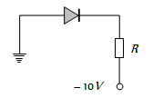
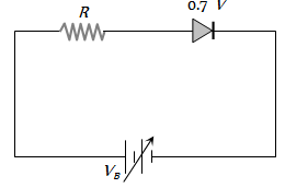
A semiconductor device is connected in a series circuit with a battery and a resistance. A current is found to pass through the circuit. If the polarity of the battery is reversed, the current drops almost to zero. The device may be

(a) A P-type semiconductor

(b) An N-type semiconductor

(c) A PN-junction

(d) An intrinsic semiconductor

Answer

(c) A PN-junction

View full question & answer
Question 521 Mark

On increasing the reverse bias to a large value in a PN-junction diode, current

(a) Increases slowly

(b) Remains fixed

(c) Suddenly increases

(d) Decreases slowly

Answer

(c) Suddenly increases

View full question & answer
Question 531 Mark

Electric current is due to drift of electrons in

(a) Metallic conductors

(b) Semi-conductors

(c) Both (a) and (b)

(d) None of these

Answer

(c) Both (a) and (b)

View full question & answer
Question 541 Mark

If ne and vd be the number of electrons and drift velocity in a semiconductor. When the temperature is increased

(a) ne increases and vd decreases

(b) ne decreases and vd increases

(c) Both ne and vd increases

(d) Both ne and vd decreases

Answer

(a) ne increases and vd decreases

View full question & answer
Question 551 Mark

A piece of semiconductor is connected in series in an electric circuit. On increasing the temperature, the current in the circuit will

(a) Decrease

(b) Remain unchanged

(c) Increase

(d) Stop flowing

Answer

(c) Increase

View full question & answer
Question 561 Mark

A hole in a P-type semiconductor is

(a) An excess electron

(b) A missing electron

(c) A missing atom

(d) A donor level

Answer

(b) A missing electron

View full question & answer
Question 571 Mark

In an insulator, the forbidden energy gap between the valence band and conduction band is of the order of      

(a) 1 MeV

(b) 0.1 MeV

(c) 1eV    

(d) 5 eV

Answer

(d) 5 eV

View full question & answer
Question 581 Mark

Bonding in a germanium crystal (semi- conductor) is

(a) Metallic

(b) Ionic

(c) Vander Waal's type

(d) Covalent

Answer

(d) Covalent

View full question & answer
Question 591 Mark

In the following circuit find I1 and I2

(a) 0, 0

(b) 5 mA, 5 mA

(c) 5 mA, 0

(d) 0, 5 mA

Answer

(d) 0, 5 mA

View full question & answer
Question 601 Mark

For a triode, at   volt, the following observations were taken, .  The value of plate resistance will be

(a) 25 kW                                           

(b) 20.8 kW

(c) 12.5 kW

(d) 100 kW

Answer

(c) 12.5 kW

View full question & answer
Question 611 Mark

Which gates is represented by this figure

(a) NAND gate

(b) AND gate

(c) NOT gate

(d) OR gate

Answer

(a) NAND gate

View full question & answer
Question 621 Mark

Which of the following gates will have an output of 1

(a)

(a)

(b)

(c)     

(d)

Answer

(c)     

View full question & answer
Question 631 Mark

For the given combination of gates, if the logic states of inputs A, B, C are as follows A = B = C = 0 and A = B = 1, C = 0 then the logic states of output D are

(a) 0, 0

(b) 0, 1 

(c) 1, 0

(d) 1, 1

Answer

(d) 1, 1

View full question & answer
Question 641 Mark

In the given figure, which of the diodes are forward biased ?

1.2.3.  4. 5.

(a) 1, 2, 3

(b) 2, 4, 5

(c) 1, 3, 4

(d) 2, 3, 4

Answer

(b) 2, 4, 5

View full question & answer
Question 651 Mark

Which of the energy band diagrams shown in the figure corresponds to that of a semiconductor

(a)


(b)

(c)

(d)

Answer

(d)

View full question & answer
Question 661 Mark

Which of the following energy band diagram shows the N-type semiconductor

(a)

(b)

(c)

(d)

Answer

(b)

View full question & answer
Question 671 Mark

The plate characteristic curve of a diode in space charge limited region is as shown in the figure. The slope of curve at point P is 5.0 mA/V. The static plate resistance of diode will be

(a) 111.1W

(b) 222.2W

(c) 333.3W

(d) 444.4W

Answer

(c) 333.3W

View full question & answer
Question 681 Mark

In the circuit given below, V(t) is the sinusoidal voltage source, voltage drop VAB(t) across the  resistance R is

(a) Is half wave rectified

(b) Is full wave rectified

(c) Has the same peak value in the positive and negative half cycles

(d) Has different peak values during positive and negative half cycle 

Answer

(d) Has different peak values during positive and negative half cycle 

View full question & answer
Question 691 Mark

In a semiconductor, the concentration of electrons is 8  and that of the holes is 5 The semiconductor  is

(a) P-type

(b) N-type

(c) Intrinsic

(d) PNP-type

Answer

(b) N-type

View full question & answer
Question 701 Mark

The diode shown in the circuit is a silicon diode. The potential difference between the points A and B will be

(a) 6 V

(b) 0.6 V

(c) 0.7 V

(d) 0 V

Answer

(a) 6 V

View full question & answer
Question 711 Mark

Ge and Si diodes conduct at 0.3 V and 0.7 V respectively. In the following figure if Ge diode connection are reversed, the valve of V0 changes by

(a) 0.2 V

(b) 0.4 V

(c) 0.6 V 

(d) 0.8 V

Answer

(b) 0.4 V

View full question & answer
Question 721 Mark

A 2V battery is connected across the points A and B as shown in the figure given below. Assuming that the resistance of each diode is zero in forward bias and infinity in reverse bias, the current supplied by the battery when its positive terminal is connected to A is

(a) 0.2 A

(b) 0.4 A

(c) Zero

(d) 0.1 A

Answer

(a) 0.2 A

View full question & answer
Question 731 Mark

Of the diodes shown in the following diagrams, which one is reverse biased

(a)

(b)

(c)

(d)

Answer

(c)

View full question & answer
Question 741 Mark

Assertion :   A P-N photodiode is made from a semiconductor for which Eg = 2.8 eV. This photo diode will not detect the wavelength of 6000 nm.

Reason    : A PN photodiode detect wavelength l if .

(a) If both assertion and reason are true and the reason is the correct explanation of the assertion.

(b) If both assertion and reason are true but reason is not the correct explanation of the assertion.

(c) If assertion is true but reason is false.

(d) If the assertion and reason both are false.

Answer

(a) If both assertion and reason are true and the reason is the correct explanation of the assertion.

View full question & answer
Question 751 Mark

Assertion  :   De-morgan's theorem   may be explained by the following circuit

Reason  :  In the following circuit, for output inputs ABC are 101

(a) If both assertion and reason are true and the reason is the correct explanation of the assertion.

(b) If both assertion and reason are true but reason is not the correct explanation of the assertion.

(c) If assertion is true but reason is false.

(d) If the assertion and reason both are false.

Answer

(c) If assertion is true but reason is false.

View full question & answer
Question 761 Mark

Assertion  :  NOT gate is also called inverter circuit.

Reason      : NOT gate inverts the input order.

(a) If both assertion and reason are true and the reason is the correct explanation of the assertion.

(b) If both assertion and reason are true but reason is not the correct explanation of the assertion.

(c) If assertion is true but reason is false.

(d) If the assertion and reason both are false.

Answer

(a) If both assertion and reason are true and the reason is the correct explanation of the assertion.

View full question & answer
Question 771 Mark

Assertion  :  Zener diode works on a principle of breakdown voltage.

Reason      : Current increases suddenly after breakdown voltage.

(a) If both assertion and reason are true and the reason is the correct explanation of the assertion.

(b) If both assertion and reason are true but reason is not the correct explanation of the assertion.

(c) If assertion is true but reason is false.

(d) If the assertion and reason both are false.

Answer

(a) If both assertion and reason are true and the reason is the correct explanation of the assertion.

View full question & answer
Question 781 Mark

Assertion : V-i characteristic of P-N junction diode is same as that of any other conductor.

Reason     : P-N junction diode behave as conductor at room temperature.

(a) If both assertion and reason are true and the reason is the correct explanation of the assertion.

(b) If both assertion and reason are true but reason is not the correct explanation of the assertion.

(c) If assertion is true but reason is false.

(d) If the assertion and reason both are false.

Answer

(d) If the assertion and reason both are false.

View full question & answer
Question 791 Mark

Assertion :   At 0 K Germanium is a superconductor. 

Reason    :    At 0 K Germanium offers zero resistance.

(a) If both assertion and reason are true and the reason is the correct explanation of the assertion.

(b) If both assertion and reason are true but reason is not the correct explanation of the assertion.

(c) If assertion is true but reason is false.

(d) If the assertion and reason both are false.

Answer

(d) If the assertion and reason both are false.

View full question & answer
Question 801 Mark

Assertion  :  NAND or NOR gates are called digital building blocks.

Reason      : The repeated use of NAND (or NOR) gates can produce all the basic or complicated gates.

(a) If both assertion and reason are true and the reason is the correct explanation of the assertion.

(b) If both assertion and reason are true but reason is not the correct explanation of the assertion.

(c) If assertion is true but reason is false.

(d) If the assertion and reason both are false.

Answer

(a) If both assertion and reason are true and the reason is the correct explanation of the assertion.

View full question & answer
Question 811 Mark

Assertion :  A transistor is a voltage-operating device.

Reason     : Base current is greater than the collector current.

(a) If both assertion and reason are true and the reason is the correct explanation of the assertion.

(b) If both assertion and reason are true but reason is not the correct explanation of the assertion.

(c) If assertion is true but reason is false.

(d) If the assertion and reason both are false.

Answer

(d) If the assertion and reason both are false.

View full question & answer
Question 821 Mark

Assertion  :  In transistor common emitter mode as an amplifier is preferred over common base mode.

Reason     : In common emitter mode the input signal is connected in series with the voltage applied to the base emitter function.

(a) If both assertion and reason are true and the reason is the correct explanation of the assertion.

(b) If both assertion and reason are true but reason is not the correct explanation of the assertion.

(c) If assertion is true but reason is false.

(d) If the assertion and reason both are false.

Answer

(b) If both assertion and reason are true but reason is not the correct explanation of the assertion.

View full question & answer
Question 831 Mark

Assertion  :  Two P-N junction diodes placed back to back, will work as a NPN transistor.

Reason     : The P-region of two PN junction diodes back to back will form the base of NPN transistor.

(a) If both assertion and reason are true and the reason is the correct explanation of the assertion.

(b) If both assertion and reason are true but reason is not the correct explanation of the assertion.

(c) If assertion is true but reason is false.

(d) If the assertion and reason both are false.

Answer

(d) If the assertion and reason both are false.

View full question & answer
Question 841 Mark

Assertion  :   Semiconductors do not Obey's Ohm's law. 

Reason     : Current is determined by the rate of flow of charge carriers.

(a) If both assertion and reason are true and the reason is the correct explanation of the assertion.

(b) If both assertion and reason are true but reason is not the correct explanation of the assertion.

(c) If assertion is true but reason is false.

(d) If assertion is false but reason is true.

Answer

(d) If assertion is false but reason is true.

View full question & answer
Question 851 Mark

Assertion :   We can measure the potential barrier of a PN junction by putting a sensitive voltmeter across its terminals.

Reason     : The current through the PN junction is not same in forward and reversed bias.

(a) If both assertion and reason are true and the reason is the correct explanation of the assertion.

(b) If both assertion and reason are true but reason is not the correct explanation of the assertion.

(c) If assertion is true but reason is false.

(d) If assertion is false but reason is true.

Answer

(d) If assertion is false but reason is true.

View full question & answer
Question 861 Mark

Assertion  :   Silicon is preferred over germanium for making semiconductor devices.

Reason      : The energy gap for germanium is more than the energy gap of silicon.

(a) If both assertion and reason are true and the reason is the correct explanation of the assertion.

(b) If both assertion and reason are true but reason is not the correct explanation of the assertion.

(c) If assertion is true but reason is false.

(d) If the assertion and reason both are false.

Answer

(c) If assertion is true but reason is false.

View full question & answer
Question 871 Mark

Assertion  : If the temperature of a semiconductor is increased then it's resistance decreases.

Reason      : The energy gap between conduction band and valence band is very small

(a) If both assertion and reason are true and the reason is the correct explanation of the assertion.

(b) If both assertion and reason are true but reason is not the correct explanation of the assertion.

(c) If assertion is true but reason is false.

(d) If the assertion and reason both are false.

Answer

(a) If both assertion and reason are true and the reason is the correct explanation of the assertion.

View full question & answer
Question 881 Mark

Assertion :   Base in a transistor is made very thin as compared to collector and emitter regions.                

Reason     : Due to thin base power gain and voltage gain is obtained by a transistor.

(a) If both assertion and reason are true and the reason is the correct explanation of the assertion.

(b) If both assertion and reason are true but reason is not the correct explanation of the assertion.

(c) If assertion is true but reason is false.

(d) If the assertion and reason both are false.

Answer

(a) If both assertion and reason are true and the reason is the correct explanation of the assertion.

View full question & answer
Question 891 Mark

Assertion : The resistivity of a semiconductor increases with temperature.

Reason     : The atoms of a semiconductor vibrate with larger amplitude at higher temperature there by increasing it's resistivity.

(a) If both assertion and reason are true and the reason is the correct explanation of the assertion.

(b) If both assertion and reason are true but reason is not the correct explanation of the assertion.

(c) If assertion is true but reason is false.

(d) If the assertion and reason both are false.

Answer

(d) If the assertion and reason both are false.

View full question & answer
Question 901 Mark

Assertion  :  A transistor amplifier in common emitter configuration has a low input impedence.

Reason      : The base to emitter region is forward biased.

(a) If both assertion and reason are true and the reason is the correct explanation of the assertion.

(b) If both assertion and reason are true but reason is not the correct explanation of the assertion.

(c) If assertion is true but reason is false.

(d) If the assertion and reason both are false.

Answer

(a) If both assertion and reason are true and the reason is the correct explanation of the assertion.

View full question & answer
Question 911 Mark

Assertion : In a common emitter transistor amplifier the input current is much less than the output current.

Reason     : The common emitter transistor amplifier has very high input impedance.

(a) If both assertion and reason are true and the reason is the correct explanation of the assertion.

(b) If both assertion and reason are true but reason is not the correct explanation of the assertion.

(c) If assertion is true but reason is false.

(d) If the assertion and reason both are false.

Answer

(c) If assertion is true but reason is false.

View full question & answer
Question 921 Mark

The given figure shows the wave forms for two inputs A and B and that for the output Y of a logic circuit. The logic circuit is

(a) An AND gate

(b) An OR gate

(c) A NAND gate

(d) An NOT gate

Answer

(a) An AND gate

View full question & answer
Question 931 Mark

A full wave rectifier circuit along with the input and output voltages is shown in the figure

Answer

(b) B, D

View full question & answer
Question 941 Mark

The slopes of anode and mutual characteristics of a triode are 0.02 mA V–1 and 1 mA V–1 respectively. What is the amplification factor of the valve

(a) 5

(b) 50

(c) 500

(d) 0.5

Answer

(b) 50

View full question & answer
Question 951 Mark

Amplification factor of a triode is 10. When the plate potential is 200 volt and grid potential is – 4 volt, then the plate current of 4mA is observed. If plate potential is changed to 160 volt and grid potential is kept at – 7 volt, then the plate current will be

(a) 1.69 mA

(b) 3.95 mA

(c) 2.87 mA

(d) 7.02 mA

Answer

(a) 1.69 mA

View full question & answer
Question 961 Mark

For a triode m = 64 and gm =1600 m mho. It is used as an amplifier and an input signal of 1V (rms) is applied. The signal power in the load of 40 kW will be

(a) 23.5 mW

(b) 48.7 mW

(c) 25.6 mW

(d) None of these

Answer

(c) 25.6 mW

View full question & answer
Question 971 Mark

A triode whose mutual conductance is 2.5 m A/volt and anode resistance is 20 kilo ohm, is used as an amplifier whose amplification is 10. The resistance connected in plate circuit will be

(a) 1 kW  

(b) 5 kW

(c) 10 kW

(d) 20 kW

Answer

(b) 5 kW

View full question & answer
Question 981 Mark

A change of 0.8 mA in the anode current of a triode occurs when the anode potential is changed by 10 V. If m = 8 for the triode, then what change in the grid voltage would be required to produce a change of 4 mA in the anode current

(a) 6.25 V

(b) 0.16 V

(c) 15.2 V

(d) None of these

Answer

(a) 6.25 V

View full question & answer
Question 991 Mark

A metallic surface with work function of 2 eV, on heating to a temperature of 800 K gives an emission current of 1 mA. If another metallic surface having the same surface area, same emission constant but work function 4 eV is heated to a temperature of 1600 K, then the emission current will be

(a) 1 mA

(b) 2 mA

(c) 4 mA

(d) None of these

Answer

(c) 4 mA

View full question & answer
Question 1001 Mark

The junction diode in the following circuit requires a minimum current of 1 mA to be above the knee point (0.7 V) of its I-V characteristic curve. The voltage across the diode is independent of current above the knee point. If VB  = 5V, then the maximum value of R so that the voltage is above the knee point, will be

(a) 4.3 kW

(b) 860 kW

(c) 4.3 W 

(d) 860 W

Answer

(a) 4.3 kW

View full question & answer