- Negative resistance.
- Where Ohm's law is obeyed.

AB: Where Ohm's law is obeyed.(Also accept BC).
12 questions · self-marked practice — reveal the answer and mark yourself.

How are these characteristics made use of in rectification?
Explanation:
In insulator, energy band gap is > 3eV.
Explanation:
In conductor, separation between conduction and valence bands is zero and in insulator, it is greater than 1eV. Hence in semiconductor the separation between conduction and valence band is 1eV.
Explanation:
According to band theory the forbidden gap in conductors $\text{E}_\text{g}\approx0$ in insulators Eg > 3eV and in semiconductors Eg < 3eV.
Explanation:
The four valence electrons of C, Si, and Ge lie respectively in the second, third and fourth orbit. Hence energy required to take out an electron from these atoms (i.e. ionisation energy Eg) will be least for Ge, followed by Si, and highest for C. Hence, the number of free electrons for conduction in Ge and Si are significant but negligibly small for C.
Light emitting diode is a photoelectric device which converts electrical energy into light energy. It is a heavily doped p-n junction diode which under forward biased emits spontaneous radiation. The general shape of the I-V characteristics of an LED is similar to that of a normal p-n junction diode, as shown. The barrier potentials are much higher and slightly different for each colour.


Explanation:
The I-V characteristics of an LED is similar to that of a Si junction diode. But the threshold voltages are much higher and slightly different for each colour.

Explanation:
As $\text{E}_\text{g}=\frac{\text{hc}}{\lambda}$
$\therefore\lambda=\frac{\text{hc}}{\text{E}_\text{g}}$
Here, Eg = 1.9ev, hc = 1240eVnm
$\therefore\lambda=\frac{1240\text{eVnm}}{1.9\text{eV}}=652.6\text{nm}$
Hence, the emitted light is of red colour.
Explanation:
A light emitting diode is a heavily doped p-n junction diode which emits light only when it is forward biased.

Explanation:
The p-n diode is forward biased when p-side is at a higher potential than n-side.
Explanation:
Forward bias resistance,
$\text{R}_1=\frac{\triangle\text{V}}{\triangle\text{I}}=\frac{0.8-0.7}{(20-10)\times10^{-6}}$
$=\frac{0.1}{10\times10^{-3}}=10$
Reverse bias resistance, $\text{R}_2=\frac{10}{1\times10^{-6}}=10^7$
Then, the ratio of forward to reverse bias resistance,
$\frac{\text{R}_1}{\text{R}_2}=\frac{10}{10^7}=10^{-6}$

Explanation:
In p-region the direction of conventional current is same as flow of holes. In n-region, the direction of conventional current is opposite to the flow of electrons.
Explanation:
In the given circuit the junction diode is forward biased and offers zero resistance.
$\therefore$ The current, $\text{I}=\frac{\text{3V-1V}}{200\Omega}=\frac{\text{2V}}{200\Omega}=0.01\text{A}.$
Explanation:
$\lambda_\text{max}=\frac{\text{hc}}{\text{E}}=\frac{6.6\times10^{-34}\times3\times10^8}{2.5\times1.6\times10^{-19}}$
= 5000Â
$\therefore\lambda=4000\widehat{\text{A}}<\lambda_\text{max}$
Explanation:
Energy of incident photon, $\text{E}=\frac{\text{hc}}{\lambda}$
$=\frac{6.6\times10^{-34}\times3\times10^8}{6\times10^{-7}\times1.6\times10^{-19}}=2.06\text{eV}$
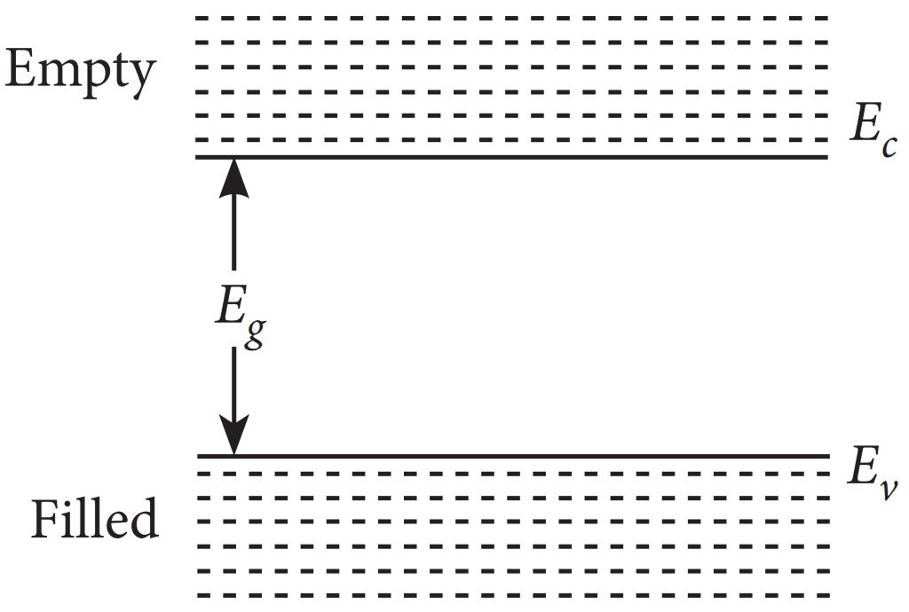
The incident radiation can be detected by a photodiode if energy of incident photon is greater than the band gap.
As D2 = 2eV, therefore D2 will detect these radiations.
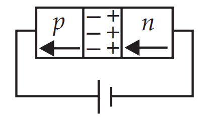
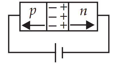
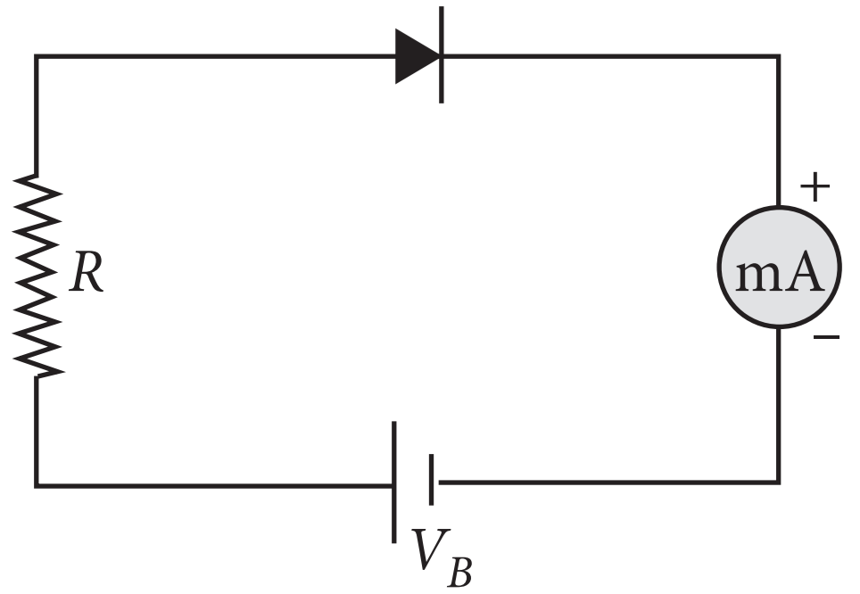
Explanation:
Photodiode is a device which is always operated in reverse bias.
Explanation:
Let Eg be the required bandwidth. Then
$\text{E}_\text{g}=\frac{\text{hc}}{\lambda}$
Here, he = 1240eV nm,
$\lambda=500\text{nm}$
$\therefore\text{E}_\text{g}=\frac{1240\text{eVnm}}{500\text{nm}}=2.48\text{eV}.$
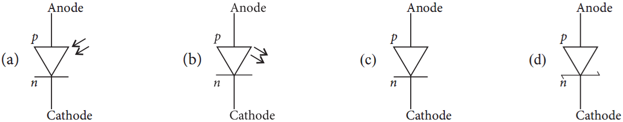
Explanation:
A photodiode is a device which is used to detect optical signals.
Explanation:
Therms value of the output voltage at the load resistance, $\frac{\text{V}_0}{\sqrt{2}}.$


Explanation:
The given circuit works as a half wave rectifier. In this circuit, we will get current through R when p-n junction is forward biased and no current when p-n junction is reverse biased. Thus the current (I) through resistor (R) will be shown in option (c).
Explanation:
$\text{E}-\frac{\text{V}_\text{B}}{\text{d}}=\frac{0.4}{4.0\times10^{-7}}$
= 1.0 × 10⁶Vm-1
Explanation:
Potential difference across = R = 3 - 0.4 = 2.6V
Resistance $\text{R}=\frac{\text{Potential difference}}{\text{Current }}$
$=\frac{2.6}{20\times10^{-3}}=130\Omega$
Explanation:
When the voltage will be the same that of the potential barrier disappears resulting in flow of current.
Explanation:
$\frac{1}{2}\text{mv}^2_1=\text{eV}_\text{B}+\frac{1}{2}\text{mv}^2_2$
$\Rightarrow\frac{1}{2}\times(9.1\times10^{-31})\times(4\times10^5)^2$
$=1.6\times10^{-19}\times(0.4)+\frac{1}{2}\times9.1\times10^{-31}\times\text{v}^2_2$
On solving, we get
v2 = 1.39 × 10⁵ms-1

Explanation:
Voltage drop across R.
VR = VB - VN= 5 - 0.7 = 4.3V
Here, Imin = 1 × 10⁻³A
$\text{R}_\text{max}=\frac{\text{V}_\text{R}}{\text{I}_\text{min}}=\frac{4.3}{1\times10^{-3}}$
$=4.3\times10^3\Omega=4.3\text{k}\Omega.$
Explanation:
I = 6mA = 6 × 10⁻³A;
VR = VB - VN= 5 - 0.7 = 4.3V
$\text{R}=\frac{\text{V}_\text{R}}{\text{I}}=\frac{4.3}{6\times10^{-3}}=717\Omega.$
Explanation:
Here, VB = 6V; VN = 0.7V,
VR = 6 - 0.7 = 5.3V
Power dissipated in R =I × VR
= (6 × 10-3) × 5.3 = 31.8 × 10⁻³W
= 31.8mW
Explanation:
Vt = Vbi + VR = 0.63 + 6 = 6.63V.
Explanation:
Diode is two terminal device, anode and cathode are the two terminals.
Explanation:
Electron concentration in n-region is more as compared to that in p-region. So electrons diffuse from n-side to p-side.
Explanation:
When an electron and a hole recombine, the energy is released in the form of light.
Explanation:
In an unbiased p-n junction, potential at p is equal to that at n.
Explanation:
The potential of depletion layer is due to ions.
Explanation:
In the depletion layer of unbiased p-n, junction has no charge carriers.
Explanation:
$\text{E}=\frac{\text{V}}{\text{l}}=\frac{2}{0.1}20\text{V/ m;}$
A = 1.0cm2 = 1.0 × 10⁻⁴m2
$\text{v}_\text{e}=\mu_\text{e}\text{E}=0.14\times20=2.8\text{ms}^{-1}$
Ie = neAeve
= ( 1.5 × 10¹⁶) × ( 1.0 × 10⁻⁴) × ( 1.6 × 10-19) × 2.8
= 6.72 × 10⁻⁷A
Explanation:
In a pure semiconductor,
ne = nh = 1.5 × 10¹⁶m-3
$\text{v}_\text{h}=\mu_\text{h}\times\text{E}=0.05\times20=1.0\text{ms}^{-1}$
Ih = nhAevh
= ( 1.5 × 10¹⁶) × ( 1.0 × 10⁻⁴) × ( 1.6 × 10-19) × 1.0
= 2.4 × 10⁻⁷A
Explanation:
$\sigma=\text{en}_\text{e}\text{m}_\text{e}$
Or $\text{n}_\text{e}=\frac{\sigma}{\text{e}\mu_\text{e}}=\frac{6.4\times10^2}{(1.6\times10^{-19}\times0.14}$
$=3.14\times10^{22}\approx3\times10^{22}\text{m}^{-3}$
Explanation:
$\text{n}_\text{e}=\frac{\text{n}^2_\text{i}}{\text{n}_\text{h}}=\frac{(1.5\times10^{16})^2}{4.5\times10^{22}}$
= 5 × 10⁹m-3
Explanation:
In case of a p-n junction diode, width of the depletion region decreases as the forward bias voltage increases.