Two amplifiers are connected one after the other in series (cascaded). The first amplifier has a voltage gain of 10 and the second has a voltage gain of 20. If the input signal is 0.01 volt, calculate the output ac signal.
Question types
Semiconductor Electronic: Material, Devices And Simple Circuits question types
474 questions across 7 question groups — pick any mix to generate a Physics paper with step-by-step answer keys.
474
Questions
7
Question groups
5
Question types
01
2 Marks Questions
51 Q→023 Marks Question
83 Q→031 Marks Question
46 Q→044 Marks Questions
12 Q→05M.C.Q (1 Marks)
214 Q→06Assertion (A) & Reason (B) MCQ
15 Q→075 Marks Questions
53 Q→Sample Questions
Semiconductor Electronic: Material, Devices And Simple Circuits questions
One sample from each question group in this chapter. Select any group above to see the full set with answer keys.
View full solution →
In half-wave rectification, what is the output frequency if the input frequency is 50 Hz. What is the output frequency of a full-wave rectifier for the same input frequency.
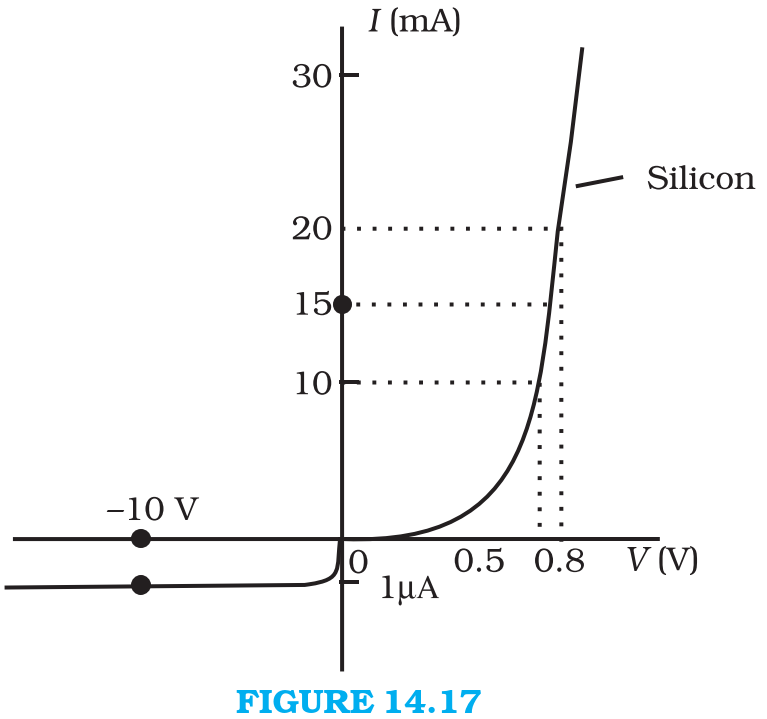
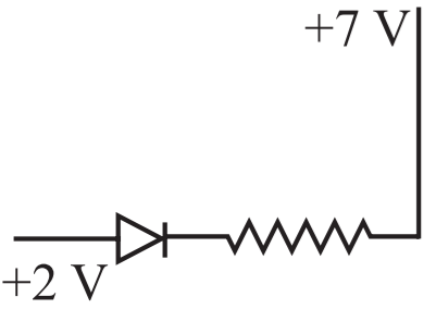
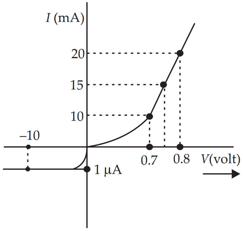
The $V-I$ characteristic of a silicon diode is shown in the Fig. 14.17. Calculate the resistance of the diode at (a) $I_D=15 mA$ and (b) $V_D=-10 V$.
View full solution →Explain, with the help of a circuit diagram, the working of a p-n junction diode as a half-wave rectifier.
Draw a circuit diagram of n-p-n transistor amplifier in CE configuration. Under what condition does the transistor act as an amplifier?
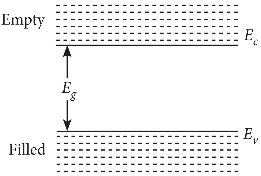
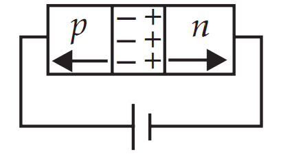
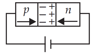
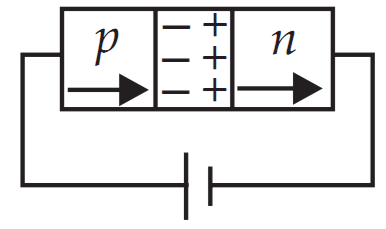
Write the two processes that take place in the formation of a p-n junction. Explain with the help of a diagram, the formation of depletion region and barrier potential in a p-n junction.
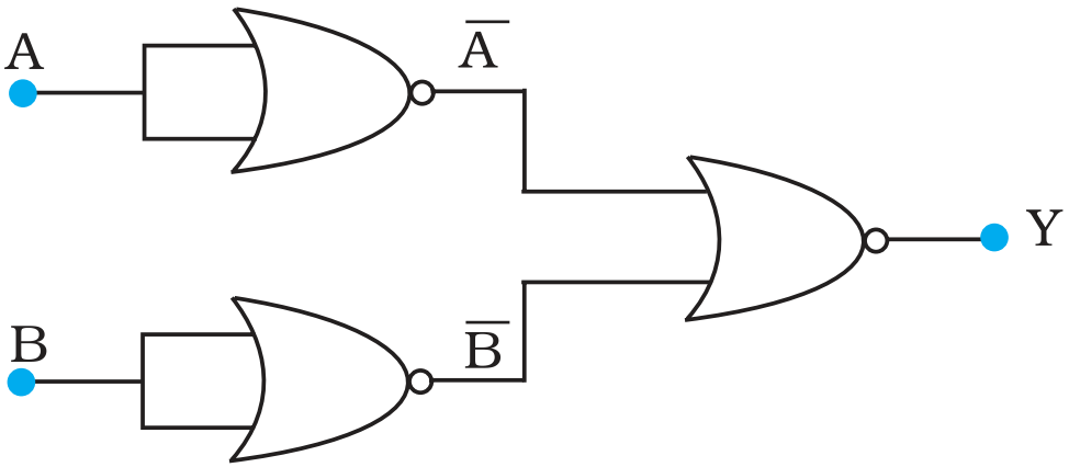
Write the truth table for circuit given in Fig. 14.47 below consisting of NOR gates and identify the logic operation (OR, AND, NOT) which this circuit is performing.
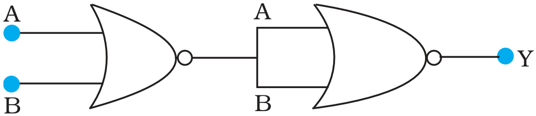
(Hint: A = 0, B = 1 then A and B inputs of second NOR gate will be 0 and hence Y=1. Similarly work out the values of Y for other combinations of A and B. Compare with the truth table of OR, AND, NOT gates and find the correct one.)
The number of silicon atoms per m3 is 5 × 1028. This is doped simultaneously with 5 × 10²² atoms per m3 of Arsenci and 5 × 10²⁰ per m3 atoms of Indium. Calculate the number of electrons and holes Given that ni = 1.5 × 10¹⁶ m-3. Is the material n-type or p-type?
Write the truth table for a NAND gate connected as given in Fig. 14.45.
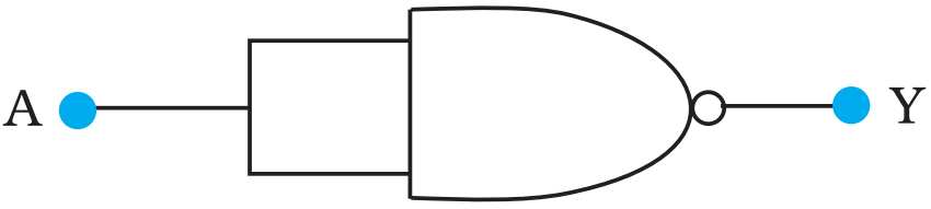
Hence identify the exact logic operation carried out by this circuit.
Hence identify the exact logic operation carried out by this circuit.
A p-n photodiode is fabricated from a semiconductor with band gap of 2.8 eV. Can it detect a wavelength of 6000 nm?
For transistor action, which of the following statements are correct:
- Base, emitter and collector regions should have similar size and doping concentrations.
- The base region must be very thin and lightly doped.
- The emitter junction is forward biased and collector junction is reverse biased.
- Both the emitter junction as well as the collector junction are forward biased.
Carbon, silicon and germanium have four valence electrons each. These are characterised by valence and conduction bands separated by energy band gap respectively equal to (Eg)C, (Eg)si and (Eg)Ge. Which of the following statements is true?
- (Eg)Si < (Eg)Ge < (Eg)C
- (Eg)C < (Eg)Ge < (Eg)Si
- (Eg)C > (Eg)Si > (Eg)Ge
- (Eg)C = (Eg)Si = (Eg)Ge
When a forward bias is applied to a p-n junction, it
- Raises the potential barrier.
- Reduces the majority carrier current to zero.
- Lowers the potential barrier.
- None of the above.
Which of the statements is true for p-type semiconductos.
- Electrons are majority carriers and trivalent atoms are the dopants.
- Electrons are minority carriers and pentavalent atoms are the dopants.
- Holes are minority carriers and pentavalent atoms are the dopants.
- Holes are majority carriers and trivalent atoms are the dopants.
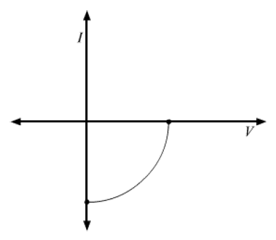
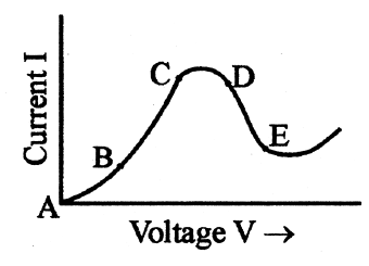
Graph showing the variation of current versus voltage for a material GaAs is shown in the figure. Identify the region of.
- Negative resistance.
- Where Ohm's law is obeyed.
- State briefly the processes involved in the formation of p-n junction explaining clearly how the depletion region is formed.
- Using the necessary circuit diagrams, show how the V-I characteristics of a p-n junction are obtained in
- Forward biasing.
- Reverse biasing.
How are these characteristics made use of in rectification?
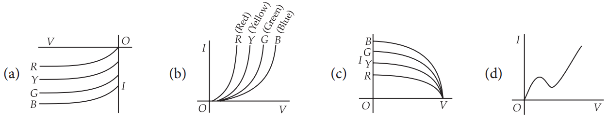
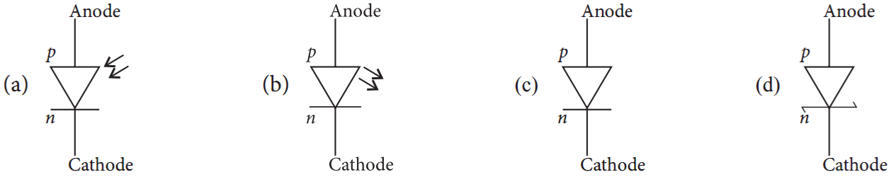
Light emitting diode is a photoelectric device which converts electrical energy into light energy. It is a heavily doped p-n junction diode which under forward biased emits spontaneous radiation. The general shape of the I-V characteristics of an LED is similar to that of a normal p-n junction diode, as shown. The barrier potentials are much higher and slightly different for each colour.
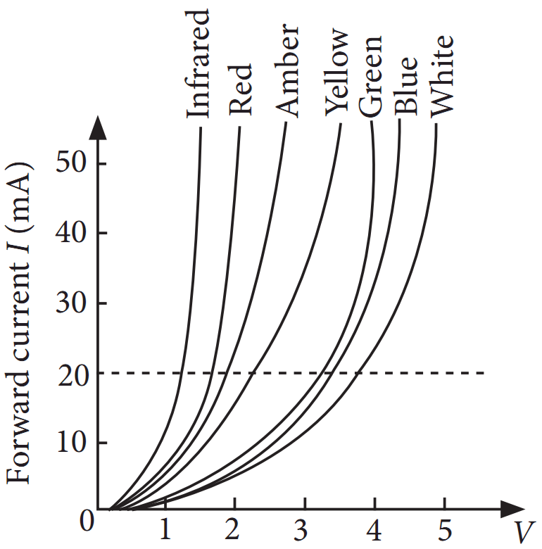
- The I-V characteristic of an LED is:
- The schematic symbol of light emitting diode is (LED).
- An LED is constructed from a p-n junction based on a certain Ga-As-P semiconducting material whose energy gap is 1.9eV. Identify the colour of the emitted light.
- Blue.
- Red.
- Violet.
- Green.
- Which one of the following statement is not correct in the case of light emitting diodes?
- It is a heavily doped p-n junction.
- It emits light only when it is forward biased.
- It emits light only when it is reverse biased.
- The energy of the tight emitted is less than the energy gap of the semiconductor used.
- The energy of radiation emitted by LED is:
- Greater than the band gap of the semiconductor used.
- Always less than the band gap of the semiconductor used.
- Always equal to the band gap of the semiconductor used.
- Equal to or less than the band gap of the semiconductor used.
There is a sudden increase in current in zener diode is:
- ADue to rupture of bonds
- BResistance of deplection layer becomes less
- CDue to high doping
- DDue to less doping
The value indicated by Fermi energy level in an intrinsic semiconductor is:
- AThe average energy of electrons and holes.
- BThe energy of electrons in conduction band.
- CThe energy of holes in valence band.
- DThe energy of forbidden region.
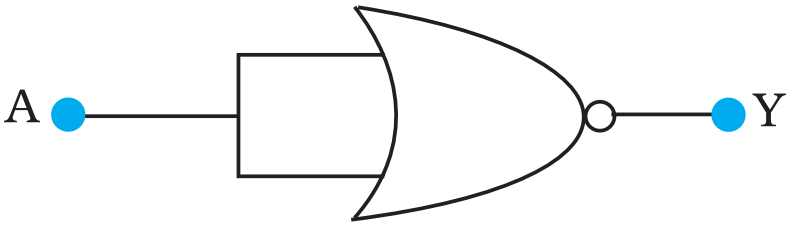
The gate that has only one input terminal:
- ANOT
- BNOR
- CNAN
- DXOR
Among the following one can act as the building blocks for the other gates is:
- ANAND and NOR
- BNAND and AND
- CXOR and OR
- DNOT and OR
Which of the following is not the function of a NOT gate?
- AStop a signal.
- BInvert an input signal.
- CComplement a signal.
- DChange the logic in a digital circuit.
Two statements are given-one labelled Assertion (A) and the other labelled Reason (R). Select the correct answer to these questions from thecodes(a), (b), (c) and (d) as given below.
- Both A and R are true and R is the correct explanation of A.
- Both A and R are true but R is not the correct explanation of A.
- A is true but R is false.
- A is false and R is also false.
Assertion: V - I characteristic of p-n diode is same as that of any other conductor.
Reason: p-n diode behave as conductor at room temperature.
Two statements are given-one labelled Assertion (A) and the other labelled Reason (R). Select the correct answer to these questions from thecodes(a), (b), (c) and (d) as given below.
Reason: Diode lasers consume less energy.
- Both A and R are true and R is the correct explanation of A.
- Both A and R are true but R is not the correct explanation of A.
- A is true but R is false.
- A is false and R is also false.
Reason: Diode lasers consume less energy.
Two statements are given-one labelled Assertion (A) and the other labelled Reason (R). Select the correct answer to these questions from thecodes(a), (b), (c) and (d) as given below.
Reason: There is a large energy gap between valence band and conduction band of diamond.
- Both A and R are true and R is the correct explanation of A.
- Both A and R are true but R is not the correct explanation of A.
- A is true but R is false.
- A is false and R is also false.
Reason: There is a large energy gap between valence band and conduction band of diamond.
Two statements are given-one labelled Assertion (A) and the other labelled Reason (R). Select the correct answer to these questions from thecodes(a), (b), (c) and (d) as given below.
Reason: The drift of electrons and holes is due to thermal excitation.
- Both A and R are true and R is the correct explanation of A.
- Both A and R are true but R is not the correct explanation of A.
- A is true but R is false.
- A is false and R is also false.
Reason: The drift of electrons and holes is due to thermal excitation.
Two statements are given-one labelled Assertion (A) and the other labelled Reason (R). Select the correct answer to these questions from thecodes(a), (b), (c) and (d) as given below.
Reason: In a semiconductor there are no free electrons at any temperature.
- Both A and R are true and R is the correct explanation of A.
- Both A and R are true but R is not the correct explanation of A.
- A is true but R is false.
- A is false and R is also false.
Reason: In a semiconductor there are no free electrons at any temperature.
Write the truth table for the circuits given in Fig. 14.48 consisting of NOR gates only. Identify the logic operations (OR, AND, NOT) performed by the two circuits.
In an intrinsic semiconductor the energy gap Eg is 1.2eV. Its hole mobility is much smaller than electron mobility and independent of temperature. What is the ratio between conductivity at 600K and that at 300K? Assume that the temperature dependence of intrinsic carrier concentration ni is given by,
$\text{n}_{\text{i}}=\text{n}_{\text{0}}\ {\text{exp}}\Big(-\frac{\text{E}_\text{g}}{2{\text{K}_{\text{B}}}{\text{T}}}\Big)$
where n0 is a constant.
View full solution →$\text{n}_{\text{i}}=\text{n}_{\text{0}}\ {\text{exp}}\Big(-\frac{\text{E}_\text{g}}{2{\text{K}_{\text{B}}}{\text{T}}}\Big)$
where n0 is a constant.
In a p-n junction diode, the current I can be expressed as,
$I=I_0\ \text{exp}\Big(\frac{\text{eV}}{2\text{k}_{\text{B}}\text{T}}-1\Big)$
where $I_0$ is called the reverse saturation current, V is the voltage across the diode and is positive for forward bias and negative for reverse bias, and $I$ is the current through the diode, kg is the Boltzmann constant (8.6×10⁻⁵ eV/K) and T is the absolute temperature. If for a given diode $I_0$ = 5×10-12 A and T = 300 K, then,
View full solution →$I=I_0\ \text{exp}\Big(\frac{\text{eV}}{2\text{k}_{\text{B}}\text{T}}-1\Big)$
where $I_0$ is called the reverse saturation current, V is the voltage across the diode and is positive for forward bias and negative for reverse bias, and $I$ is the current through the diode, kg is the Boltzmann constant (8.6×10⁻⁵ eV/K) and T is the absolute temperature. If for a given diode $I_0$ = 5×10-12 A and T = 300 K, then,
- What will be the forward current at a forward voltage of 0.6V?
- What will be the increase in the current if the voltage across the diode is increased to 0.7V?
- What is the dynamic resistance?
- What will be the current if reverse bias voltage changes from 1V to 2V?
- Describe briefly, with the help of a diagram, the role of the two important processes involved in the formation of a p-n junction.
- Name the device which is used as a voltage regulator. Draw the necessary circuit diagram and explain its working.
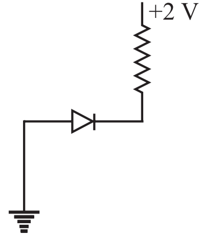
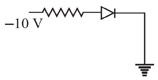
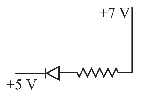
- Draw the circuit diagrams of a p-n junction diode in (i) forward bias, (ii) reverse bias. How are these circuits used to study the V - I characteristics of a silicon diode? Draw the typical V - I characteristics.
- What is a light emitting diode (LED)? Mention two important advantages of LEDs over conventional lamps.
Generate a Semiconductor Electronic: Material, Devices And Simple Circuits paper free
Pick question groups from the list above, set marks and difficulty, and export a branded PDF with step-by-step answer keys. First 3 chapters free — no signup.