Of the diodes shown in the following diagrams, which one is reverse biased
- A
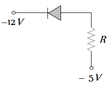
- B
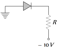
- C
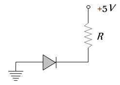
- D
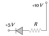
[CBSE PMT 2004]


Download our appand get started for free
Experience the future of education. Simply download our apps or reach out to us for more information. Let's shape the future of learning together!No signup needed.*
Similar Questions
- 1A piece of copper and the other of germanium are cooled from the room temperature to $80 K$, then which of the following would be a correct statementView Solution
- 2For a transistor, the current amplification factor is $0.8.$ The transistor is connected in common emitter configuration. The change in the collector current when the base current changes by 6 $m A$ isView Solution
- 3View SolutionIn a semiconductor the separation between conduction band and valence band is of the order of
- 4View SolutionThe part of a transistor which is heavily doped to produce a large number of majority carriers, is
- 5View SolutionThe unit of mutual conductance of a triode valve is
- 6In a full wave rectifiers, input $a c$ current has a frequency ' $v$. The output frequency of current isView Solution
- 7View SolutionThe most commonly used material for making transistor is
- 8Carbon, silicon and Germanium atoms have four valence electrons each. Their valence and conduction band are separated by energy band gaps represented by $(E) .(E)$ and $(E)$ respectively. Which one of the following relationship is true in their caseView Solution
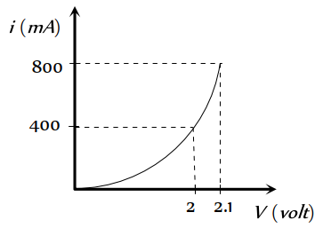
- 9The $i-V$ characteristic of a $P-N$ junction diode is shown below. The approximate dynamic resistance of the $P-N$ junction when a forward bias of $2$ volt is appliedView Solution
- 10The energy gap of silicon is $1.14\ eV$. The maximum wavelength at which silicon will begin absorbing energy isView Solution