Which of the energy band diagrams shown in the figure corresponds to that of a semiconductor
- A
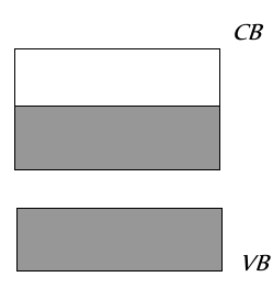
- B
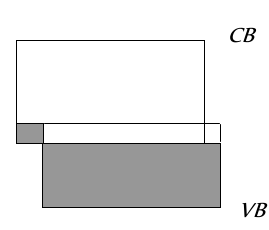
- C
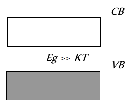
- D
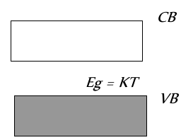
[Orissa JEE 2003]


Download our appand get started for free
Experience the future of education. Simply download our apps or reach out to us for more information. Let's shape the future of learning together!No signup needed.*
Similar Questions
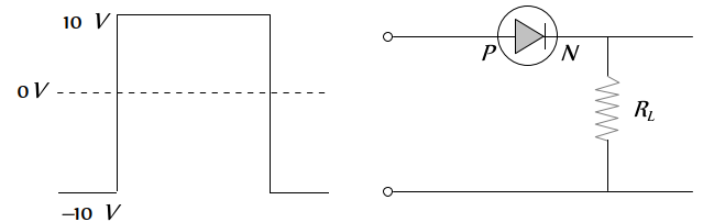
- 1If the following input signal is sent through a $P N$-junction diode, then the output signal across $R$ will beView Solution
- 2The current through an ideal $P N$-junction shown in the following circuit diagram will beView Solution
- 3View SolutionIn comparison to a half wave rectifier, the full wave rectifier gives lower
- 4View SolutionThe electrical circuits used to get smooth d.c. output from a rectifier circuit is called
- 5In a common emitter transistor, the current gain is $80.$ What is the change in collector current, when the change in base current is $250 \mu A$View Solution
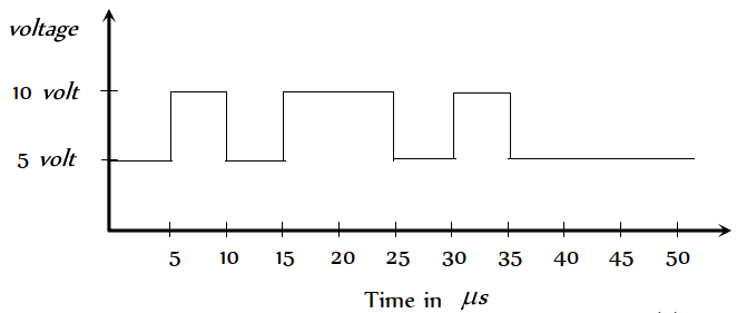
- 6View SolutionIn a negative logic the following wave form corresponds to the
- 7A semiconductor $X$ is made by doping a germanium crystal with arsenic $(Z=33)$. A second semiconductor $Y$ is made by doping germanium with indium $(Z=49)$. The two are joined end to end and connected to a battery as shown. Which of the following statements is correctView Solution
- 8View SolutionA crystal diode is a
- 9For a thermionic emitter (metallic) if $J$ represents the current density and $T$ is its absolute temperature then the correct curve between $\log _e \frac{J}{T^2}$ and $\frac{1}{T}$ isView Solution
- 10On increasing the reverse bias to a large value in a $P N$-junction diode, currentView Solution