The current through an ideal $P N$-junction shown in the following circuit diagram will be
[AMU 1998]


Download our appand get started for free
Experience the future of education. Simply download our apps or reach out to us for more information. Let's shape the future of learning together!No signup needed.*
Similar Questions
- 1The cause of the potential barrier in a $P-N$ diode isView Solution
- 2View SolutionDonor type impurity is found in
- 3View SolutionThe thermionic emission of electron is due to
- 4If the two ends $P$ and $N$ of a $P-N$ diode junction are joined by a wireView Solution
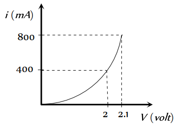
- 5The $i-V$ characteristic of a $P-N$ junction diode is shown below. The approximate dynamic resistance of the $P-N$ junction when a forward bias of $2$ volt is appliedView Solution
- 6The depletion layer in the $P-N$ junction region is caused byView Solution
- 7View SolutionRegarding a semiconductor which one of the following is wrong
- 8If the amplification factor of a triode $(\mu)$ is 22 and its plate resistance is $6600 ohm$, then the mutual conductance of this valve is mho isView Solution
- 9In NPN transistor the collector current is $10\ mA$. If $90 \%$ of electrons emitted reach the collector, thenView Solution
- 10In a common emitter transistor, the current gain is $80.$ What is the change in collector current, when the change in base current is $250 \mu A$View Solution